Pulse width modulation inverter circuit and control method thereof
- Summary
- Abstract
- Description
- Claims
- Application Information
AI Technical Summary
Benefits of technology
Problems solved by technology
Method used
Image
Examples
Embodiment Construction
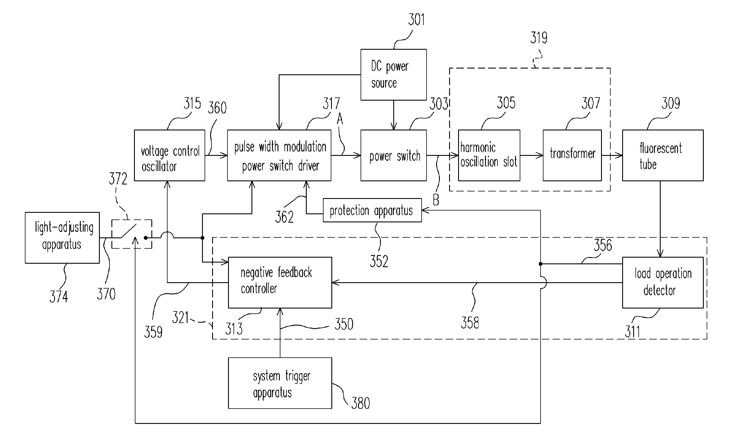
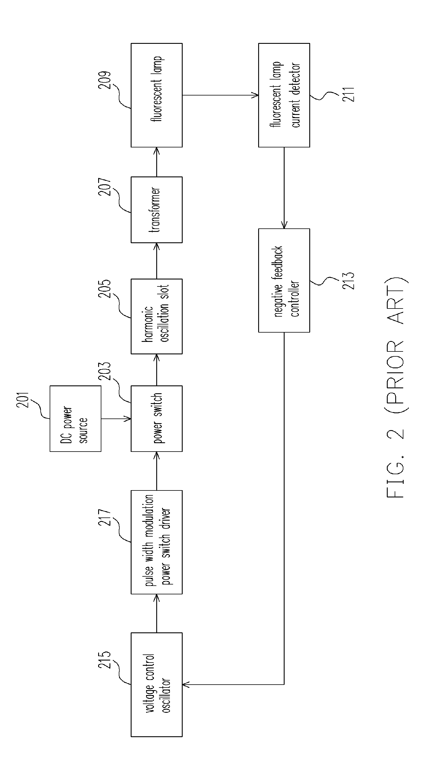
[0037]FIG. 3 is a circuit block diagram showing an inverter circuit according to an embodiment of the present invention. Referring to FIG. 3, different from the traditional inverter circuit, the embodiment of the present invention replaces the fixed pulse width power switch driver of the traditional circuit with the pulse width modulation power switch driver 317. The pulse width modulation power switch driver 317 receives the voltage from the DC power source 301 to determine the output pulse width.
[0038] When the circuit starts operation, after receiving the voltage of the DC power source 301, the pulse width modulation power switch driver 317 outputs the pulse width modulation signal according to the voltage of the DC power source 301. The power switch 303 determines its own turn-on time period according to the pulse width of the pulse width modulation signal. The power switch 303 also outputs a signal from the DC power source 301 to transmit the voltage of the DC power source 301...
PUM
 Abstract
Description
Claims
Application Information


