Current collimation for thin seed and direct plating

a technology of direct plating and thin seed, which is applied in the field of current collimation of thin seed and direct plating, can solve the problems of high resistance and thin conductive seed layer formed on the substra

Inactive Publication Date: 2006-05-18
APPLIED MATERIALS INC
View PDF96 Cites 14 Cited by
  • Summary
  • Abstract
  • Description
  • Claims
  • Application Information

AI Technical Summary

Problems solved by technology

However, with conventional ECP processes and systems, the conductive seed layer formed on the substrate is generally very thin, and as such, is highly resistive.
This phenomenon is generally known as the “terminal effect”, and is an undesirable characteristic associated with conventional plating systems.

Method used


Image

  • Current collimation for thin seed and direct plating
  • Current collimation for thin seed and direct plating
  • Current collimation for thin seed and direct plating

Examples


Embodiment Construction

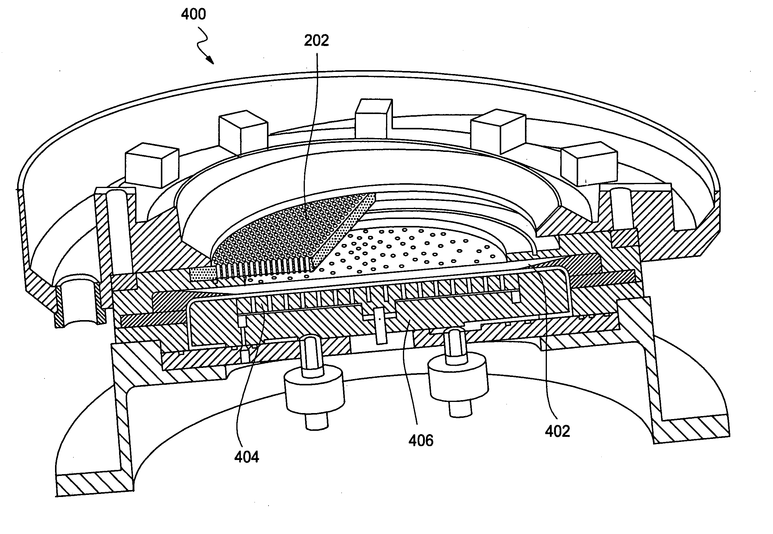
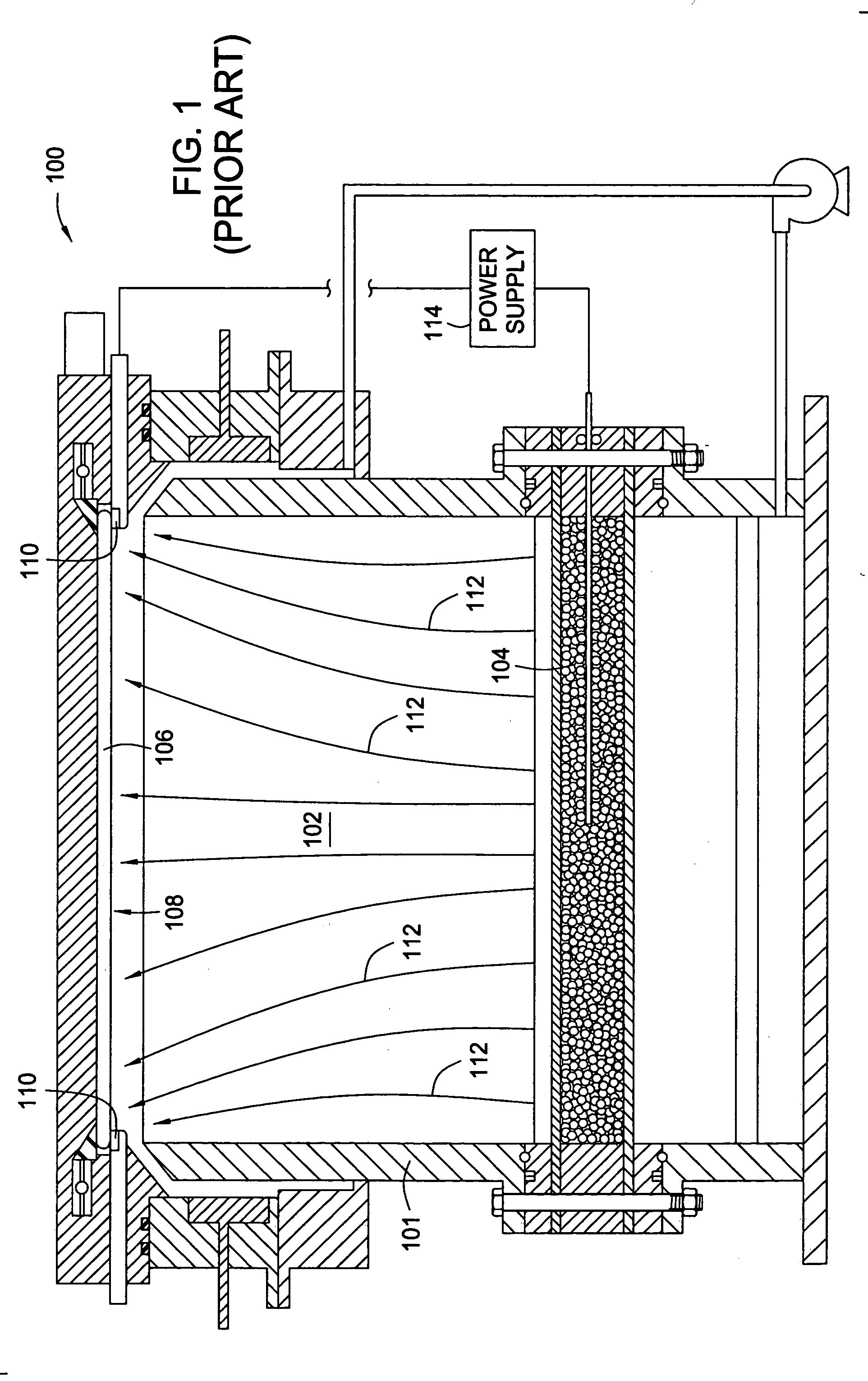
[0027]FIG. 1 illustrates a schematic view of a conventional plating cell 100 and the electric field lines generated therein. The conventional plating cell 100 generally includes a fluid basin 101 configured to contain a fluid volume 102, which is generally an electrolyte plating solution. An anode 104 is positioned in a lower portion of the fluid basin 101 and a substrate 106 that is to be plated is generally positioned across an upper open portion of the cell 100. The substrate 106 is supported by a contact ring that is configured to electrically contact the plating surface 108 of the substrate 106 near the perimeter of the substrate 106 via one or more electric contact elements 110. The electric contact elements 110 are in electrical communication with a cathodic terminal of a power supply 114, while the anodic terminal of the power supply is in electrical communication with the anode 104. Further details of the conventional plating cell 100 may be found in commonly assigned U.S. ...


PUM

PropertyMeasurementUnit
interior diameteraaaaaaaaaa
inner diameteraaaaaaaaaa

Abstract

A method and apparatus for plating a conductive material onto a substrate is provided. The apparatus includes a fluid processing cell having a fluid basin configured to contain an electrolyte solution and having an opening configured to receive a substrate for processing, an anode assembly positioned in the fluid basin, and a collimator positioned in the fluid basin between the anode assembly and the opening.

Description

BACKGROUND OF THE INVENTION [0001] 1. Field of the Invention [0002] Embodiments of the invention generally relate to an electrochemical plating cell having an electric field collimator positioned between the anode and the substrate being plated. [0003] 2. Description of the Related Art [0004] In semiconductor processing, electrochemical plating (ECP) is generally the preferred technique for filling features formed onto substrates with a conductive material. A typical ECP process generally includes immersing a substrate into an electrolyte solution that is rich in ions of the conductive material (generally copper), and then applying an electrical bias between a conductive seed layer formed on the surface of the substrate and an anode positioned in the electrolyte solution. The application of the electrical bias between the seed layer and the anode facilitates an electrochemical reaction that causes the ions of the conductive material to plate onto the seed layer. [0005] However, with...

Claims


Application Information

Patent Timeline
Patent Type & Authority Applications(United States)
IPC IPC(8): C25C3/16C25B9/00C25D17/00
CPCC25D7/123C25D17/001C25D17/008C25D17/007
Inventor HERCHEN, HARALDDUKOVIC, JOHN O.PANG, LILY
Owner APPLIED MATERIALS INC
Why Eureka
Try Eureka