Carrier for substrate film

a film carrier and substrate technology, applied in the field of substrate film carriers, can solve the problems of affecting the processing efficiency of substrate films, so as to enhance the rigidity of substrate films and enhance the rigidity of substrate units

Inactive Publication Date: 2006-05-18
DICKEY BRENTON L
View PDF73 Cites 0 Cited by
  • Summary
  • Abstract
  • Description
  • Claims
  • Application Information

AI Technical Summary

Benefits of technology

[0008] The invention relates to a carrier for supporting a substrate film during the chip-substrate assembly and bonding process. The carrier provides enhanced rigidity to the substrate film. The degree of rigidity and / or flexibility provided can be controlled by selection of the carrier dimensions, configuration and material choice. Advantages of embodiments of the carrier include easier handling, reduced probability of defective end products, and increased control in choosing the thinness of the substrate film. For example, the substrate film carrier can be used for lead-over-chip (LOC) assemblies and lead-under-chip (LUC) assemblies to create ball grid arrays (BGA), pin grid arrays (PGA), dual in-line packages (DIP), and the like.
[0009] In one embodiment, a carrier for supporting a substrate film comprises side bars and cross bars. The side bars and cross bars are in mechanical communication with the substrate film and provide rigidity during the manufacturing process. In another embodiment, an assembly comprises a substrate film and a carrier. The carrier comprises side bars which are in mechanical communication with the substrate film.
[0010] In another embodiment, an assembly comprises a film and a carrier. The film includes a plurality of substrate units. The plurality of substrate units is adapted to electrically interface with a plurality of dies. The carrier is in mechanical communication with the film. The carrier provides enhanced rigidity to the film by being sized and configured to add material at selected regions of the film.

Problems solved by technology

But this thinness can also cause the substrate film reel to be fragile and flimsy.
As a result, during the assembly process, the film is prone to undesirable and / or unwanted bending and movement.
This cannot only cause damage to the die, the substrate and the die-substrate interface, but can also complicate the handling and assembly of the die and substrate.
For example, undesirable bending of the film substrate can result in breakage of one or more of the leads connecting the dies to the substrate.

Method used


Image

  • Carrier for substrate film
  • Carrier for substrate film
  • Carrier for substrate film

Examples


Embodiment Construction

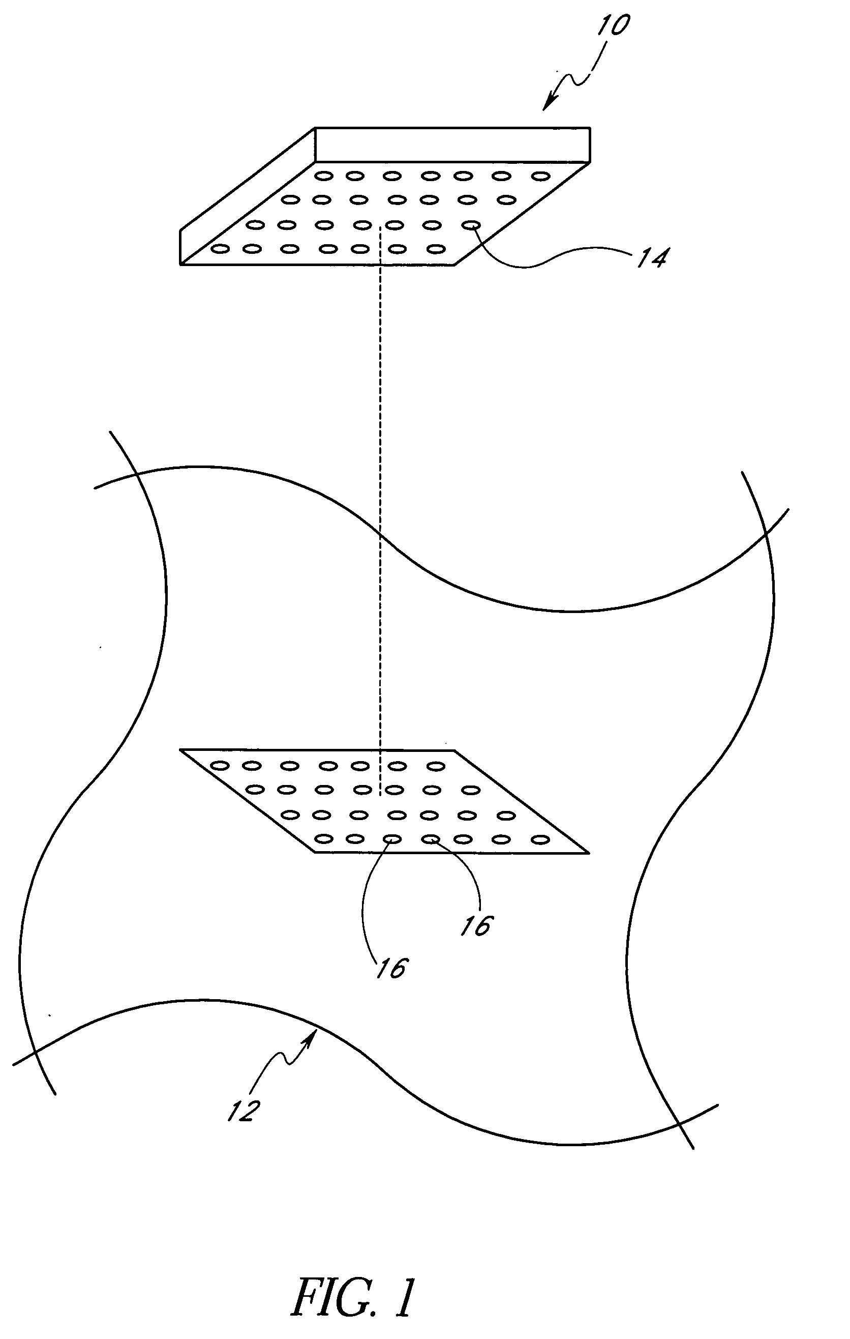
[0025]FIG. 1 schematically illustrates a ball grid array (BGA) chip package 10 and a printed circuit board (PCB) 12. The BGA package 10 serves as an encapsulating device for a die or chip and permits electrical access to the die via solder or electrode bumps 14. The PCB 12 includes a pattern of pads 16 which are arranged in alignment with the BGA solder bumps 14. This allows the BGA chip package 10 to be connected to the PCB 12. Of course, other chip packaging types may also be used, for example, pin grid arrays (PGA), dual in-line packages (DIP), and the like. These packaging types can be connected to compatible connectors on a PCB or other external circuitry.

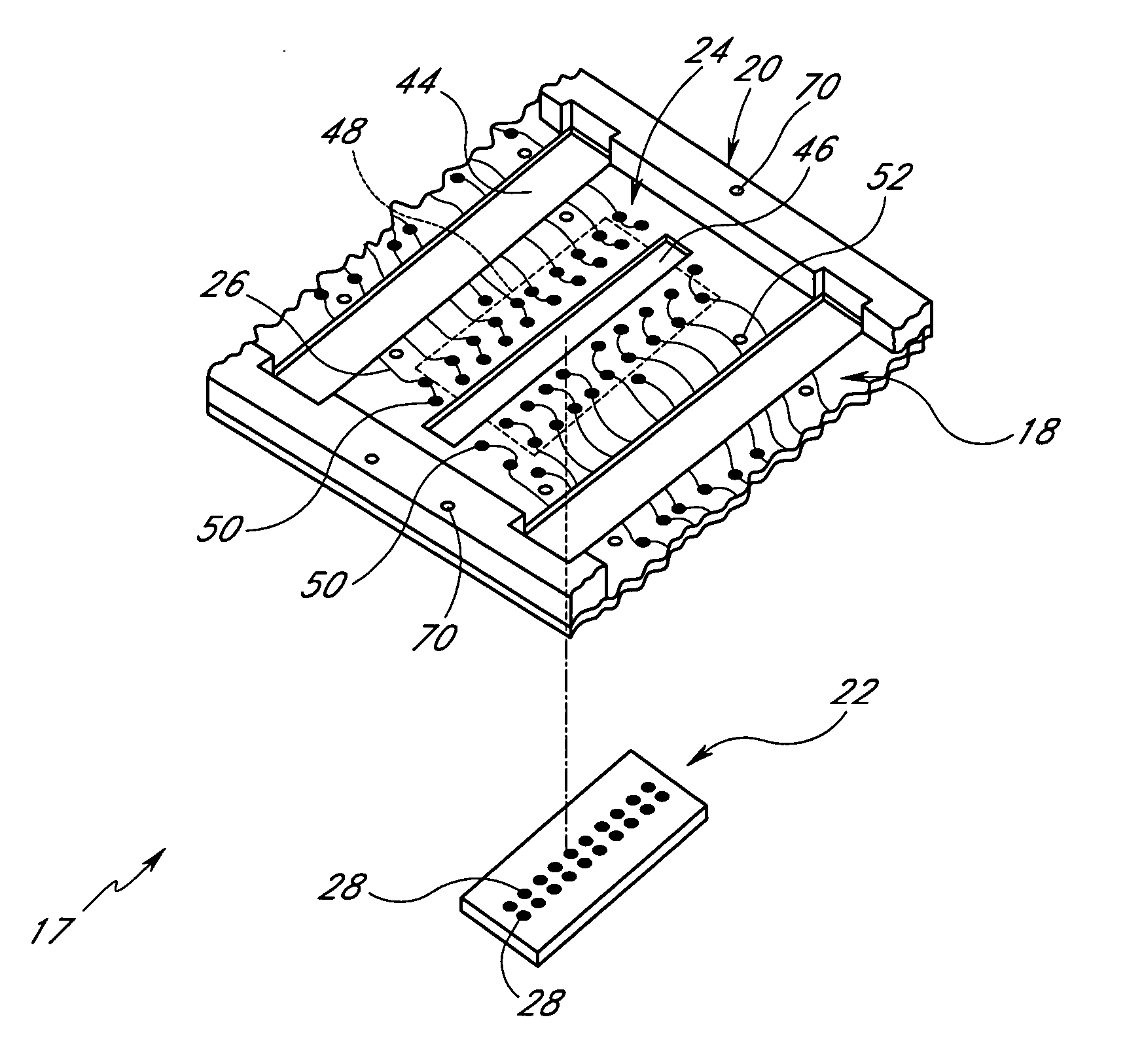
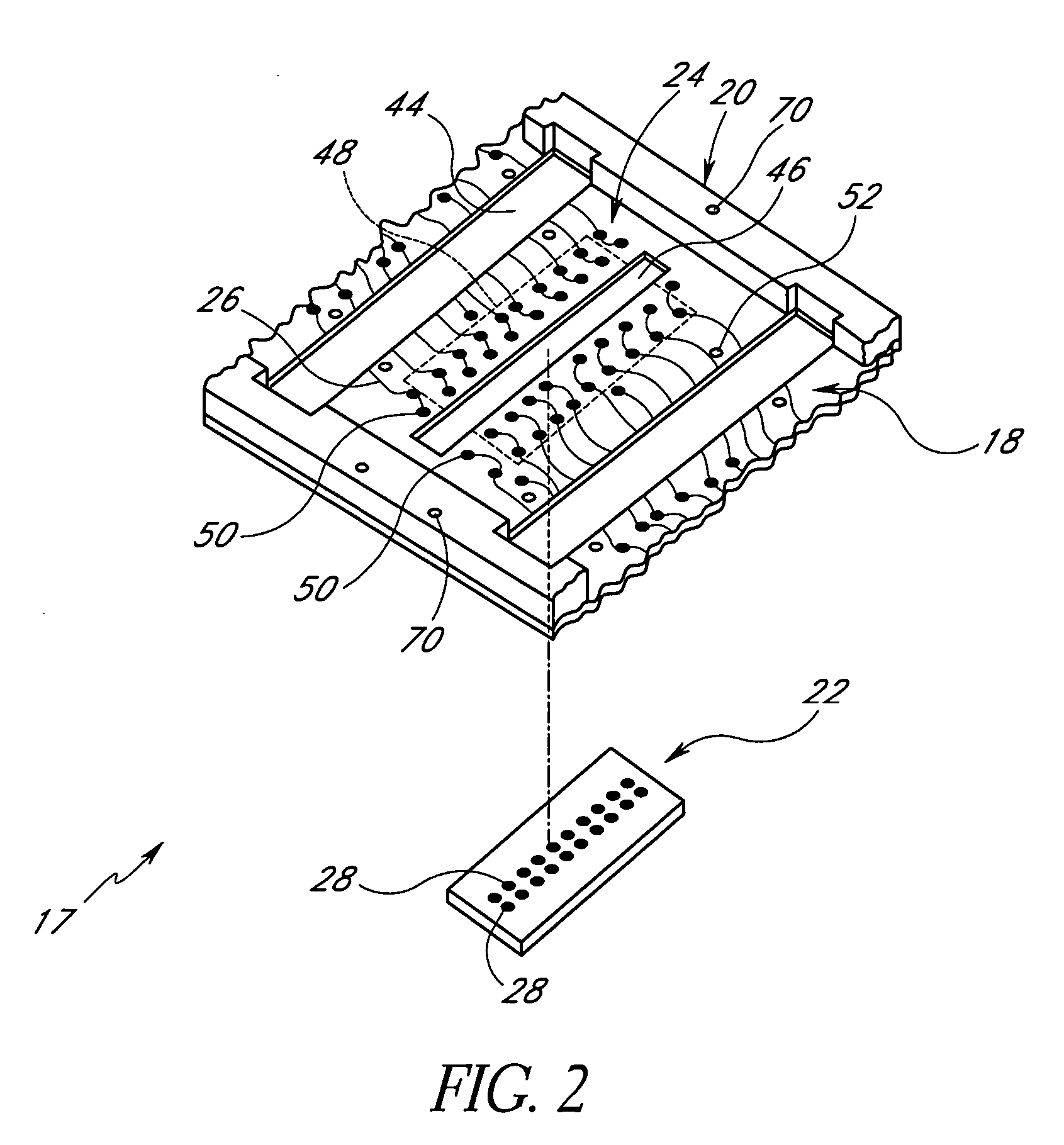
[0026] In accordance with one embodiment, FIG. 2 is a representation of a lead-over-chip (LOC) assembly 17 and generally shows a substrate film 18, a film carrier or structure 20 and a semiconductor die or chip 22. The substrate film 18 includes a plurality of substrate units 24, as discussed in greater detail below, with eac...


PUM


Abstract

The invention relates to a carrier for supporting a substrate film during the chip-substrate assembly and bonding process. The carrier provides enhanced rigidity to the substrate film. The degree of rigidity and / or flexibility provided can be controlled by selection of the carrier dimensions, configuration and material choice. Advantages of embodiments of the carrier include easier handling, reduced probability of defective end products, and increased control in choosing the thinness of the substrate film. For example, the substrate film carrier can be used for lead-over-chip (LOC) assemblies and lead-under-chip (LUC) assemblies to create ball grid arrays (BGA), pin grid arrays (PGA), dual in-line packages (DIP), and the like.

Description

RELATED APPLICATION(S) [0001] This application is a continuation of U.S. patent application Ser. No. 09 / 389,720, filed Sep. 3, 1999, the entirety of which is hereby incorporated by reference herein.BACKGROUND OF THE INVENTION [0002] 1. Field of the Invention [0003] The present invention relates generally to the handling of semiconductor chips and, specifically, to a carrier adapted for supporting a substrate film during the assembly and bonding process. [0004] 2. Description of the Related Art [0005] In today's integrated circuit (IC) technology, semiconductor chips or dies are typically batch fabricated on a silicon wafer. The wafer may contain hundreds of dies arranged in a matrix. The dies are separated and each die is typically mounted on an appropriate substrate, contacted, and packaged. [0006] The substrate is typically a thin flexible tape or film reel which permits automated transport and handling of the dies. Many dies may be attached adjacently to a single tape using, for ...

Claims


Application Information

Patent Timeline
Patent Type & Authority Applications(United States)
IPC IPC(8): H01L23/495H05K1/00H05K3/00
CPCH01L21/6835H01L23/13H01L23/4951H01L23/49572H01L23/4985H01L23/544H01L24/85H01L2224/85203H01L2224/85205H01L2924/01079H01L2924/14H05K1/0393H05K3/0097H01L24/83H01L2924/01029H01L2924/10253H01L2924/00H01L2224/83H01L2924/00014H01L2224/48H01L24/45H01L24/48H01L2224/45124H01L2224/45144H01L2224/45015H01L2924/207
Inventor DICKEY, BRENTON L.
Owner DICKEY BRENTON L
Why Eureka
Try Eureka