Module substrate and disk apparatus

Inactive Publication Date: 2006-05-18
KK TOSHIBA
View PDF10 Cites 28 Cited by
  • Summary
  • Abstract
  • Description
  • Claims
  • Application Information

AI Technical Summary

Problems solved by technology

However, while injecting the resin solution for forming underfill, the resin solution, in some cases, flows out from the region where the active element parts of the printed wiring board are mounted to spread to peripheral parts, and therefore the following problems may occur.
That is, for example, in a module substrate that uses a printed wiring board in which a rigid insulating substrate made of an epoxy resin as its main material is built, the spreading of the underfill to peripheral parts creates

Method used


Image

  • Module substrate and disk apparatus
  • Module substrate and disk apparatus
  • Module substrate and disk apparatus

Examples


first embodiment

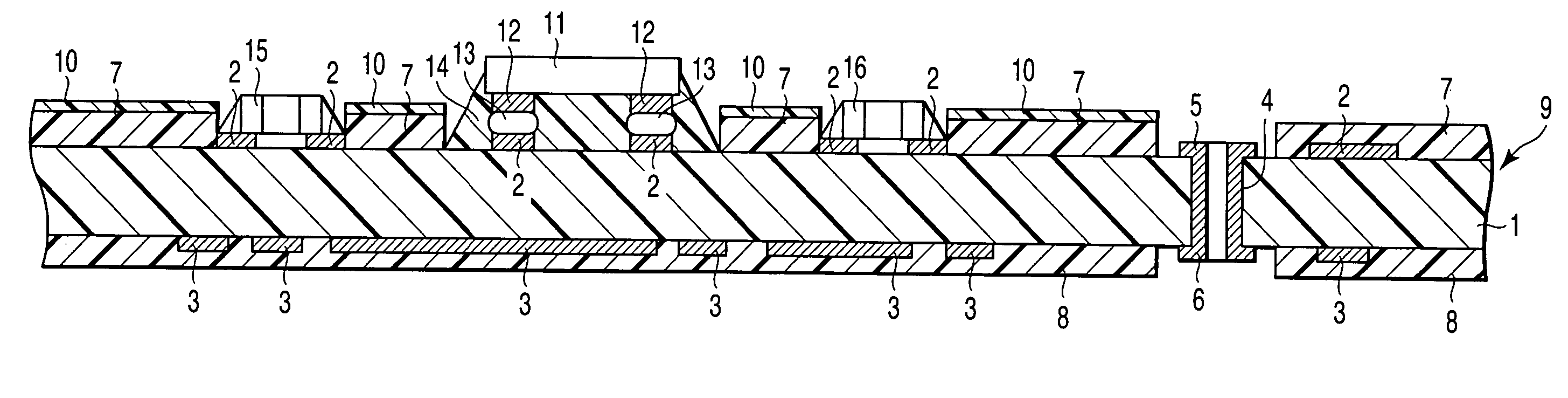
[0017]FIG. 1 is an exemplary diagram showing a cross section of a module substrate equipped with a printed wiring board including a rigid insulating substrate, according to the first embodiment of the present invention.

[0018] A rigid insulating substrate 1, which is made of, for example, a glass epoxy resin, has circuits patterns 2 and 3 formed on top and bottom surfaces, respectively. A through-hole 4 is formed to be through the rigid insulating substrate 1. Lands 5 and 6 are formed in vicinities of openings at both ends of the through hole 4, respectively. Solder resist films 7 and 8, which serve as protection films, are formed on the top and bottom surfaces of the rigid insulating substrate 1 to cover the circuit patterns 2 and 3, respectively. The solder resist film 7 formed on the top surface side has openings at portions of the circuit pattern 2 where parts of active elements and passive elements are mounted, and at a section of the land 5. The solder resist film 8 formed on ...

second embodiment

[0033]FIG. 3 is an exemplary diagram showing a cross section of a module substrate equipped with a flexible printed wiring board including a flexible insulating substrate, according to the second embodiment of the present invention.

[0034] A flexible insulating substrate 31 made of, for example, polyimide, has an opening portion 32 formed regionally. A circuit pattern having a layered structure of, for example, Cr / Cu and Cu is formed on a top surface of the flexible insulating substrate 31, and a backing plate 34 made of, for example, SUS is formed on a bottom surface (at least a section corresponding to an active element part, which will be described later). Exposed surfaces of the circuit pattern 33 are each covered with, for example, a Ni thin film 35. A coverlay 36 made of, for example, polyimide, which serves as a protective film, is formed on the flexible insulating substrate 31 that includes the circuit pattern 33. The coverlay 36 has openings each at a section corresponding ...

third embodiment

[0050]FIG. 5 is an exemplary perspective view showing a hard disk drive (to be called HDD hereinafter) serving as a disk apparatus according to a third embodiment of the present invention, and FIG. 6 is an exemplary perspective view showing a flexible module substrate shown in FIG. 5.

[0051] As shown in FIG. 5, the HDD includes a case 61 having a rectangular box shape with an upper surface opened, and a top cover to open / close the opened upper end of the case, which is fixed to the case with a plurality of screws.

[0052] The case 61 contains two magnetic disks 62a and 62b serving as recording media, a spindle motor 63 serving as a drive member for supporting and rotating these magnetic disks, a plurality of magnetic heads that record data on a magnetic disk or reproduce data therefrom, a head actuator 64 that supports these magnetic heads to be movable with respect to the magnetic disks 62a and 62b, a voice coil motor (to be called VCM hereinafter) that rotationally moves and positi...


PUM

PropertyMeasurementUnit
Thicknessaaaaaaaaaa
Flexibilityaaaaaaaaaa

Abstract

A module substrate includes an insulating substrate, a circuit pattern formed on at least a main surface of the insulating substrate, a protection film formed on the main surface of the insulating substrate including the circuit patter such as to expose a mount region of the circuit pattern, an active element part mounted on the mount region of the circuit pattern, a fluororesin film formed on the protection film at least in a vicinity of the mount region of the active element part, and an underfill filled between the active element part and the mount region of the circuit pattern.

Description

CROSS-REFERENCE TO RELATED APPLICATIONS [0001] This application is based upon and claims the benefit of priority from prior Japanese Patent Application No. 2004-331979, filed Nov. 16, 2004, the entire contents of which are incorporated herein by reference. BACKGROUND OF THE INVENTION [0002] 1. Field of the Invention [0003] One embodiment of the present invention relates to a module substrate and disk apparatus. [0004] 2. Description of the Related Art [0005] As a conventionally known substrate, there is a module substrate in which active element parts including bare chips are mounted in a circuit pattern of a printed wiring board. When mounting active element parts in the circuit pattern of the print wiring board in the conventional module substrate, first, the electrodes of the active element parts are soldered to the circuit pattern of the printed wiring board. Then, a resin solution for formation of underfill is injected between the printed wiring board and the active element par...

Claims


Application Information

Patent Timeline
IPC IPC(8): H01L23/48
CPCG11B25/043G11B5/4846H01L24/16H01L24/28H01L24/32H01L2224/13099H01L2224/16225H01L2224/16237H01L2224/27013H01L2224/73203H01L2224/83051H01L2224/83102H01L2224/92125H01L2924/01005H01L2924/01009H01L2924/01029H01L2924/01033H01L2924/01078H01L2924/01079H01L2924/15153H01L2924/1517H01L2924/19041H01L2924/19043H01L2924/19105H05K3/28H05K3/284H05K2201/015H05K2201/0195H05K2201/10674H05K2201/10977H01L2924/01006H01L2924/01019H01L2924/01023H01L2924/01024H01L2924/014H01L21/563H01L2224/05573H01L2224/05568H01L2924/00014H01L2224/0554H01L2224/05599H01L2224/0555H01L2224/0556
Inventor AOKI, MAKOTOHOSODA, KUNIYASU
Owner KK TOSHIBA
Why Eureka
Try Eureka