

Diode array architecture for addressing nanoscale resistive memory arrays
a resistive memory array and diode array technology, applied in the field of memory devices, can solve problems such as the breakdown of diodes
- Summary
- Abstract
- Description
- Claims
- Application Information
AI Technical Summary
Benefits of technology
Problems solved by technology
Method used
Image

Examples
Embodiment Construction
[0029] Reference is now made in detail to a specific embodiment of the present invention which illustrates the best mode presently contemplated by the inventors for practicing the invention.
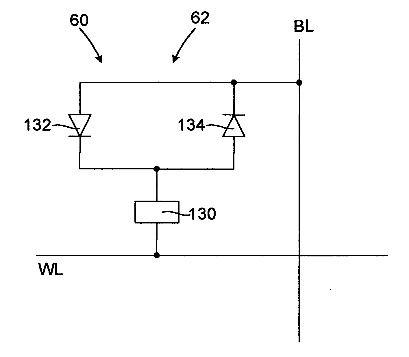
[0030]FIG. 7 illustrates an embodiment of the present invention. A conductor BL is shown therein, and a conductor WL overlies, crosses and is spaced from the conductor BL. A structure 60 interconnects the conductor BL and the conductor WL at the intersection thereof. The structure 60 includes a resistive memory cell 130, similar to the resistive memory cell 30 above, connected to the conductor WL, a first diode 132 connected to the resistive memory cell 130 and the conductor BL, and a second diode 134 also connected to the resistive memory cell 130 and the conductor BL, in parallel with the first diode 132. The first diode 132 is oriented in the forward direction from the resistive memory cell 130 to the conductor BL, and the second diode 134 is oriented in the reverse direction from the resisti...
PUM
 Abstract
Description
Claims
Application Information