Solid-state image-sensing device

a solid-state image and image-sensing technology, applied in the field of solid-state image-sensing devices, can solve the problems of narrow dynamic range, flat blackness in dim portions of obtained images, and saturation in bright portions, and achieve the effect of accurate compensation data acquisition

Inactive Publication Date: 2006-06-08
SONY SEMICON SOLUTIONS CORP
View PDF3 Cites 5 Cited by
  • Summary
  • Abstract
  • Description
  • Claims
  • Application Information

AI Technical Summary

Benefits of technology

[0010] An object of the present invention is to provide a solid-state image-sensing device that, without requiring irradiation of uniform light beforehand, permits accurate acquisition of compensation data to be used to correct the outputs from individual pixels during shooting of a subject.
[0011] Another object of the present invention is to provide a solid-state image-sensing device in which variations in sensitivity among pixels are minimized by making the initial states of the individual pixels substantially identical.
[0012] Still another object of the present invention is to provide a solid-state image-sensing device that permits shooting of a subject having a wide brightness range, i.e. a subject of which the brightness ranges from low to high, with high resolution.

Problems solved by technology

A CCD-type image-sensing device accumulates photoelectric charges in potential wells while transferring them, and has the disadvantage of a comparatively narrow dynamic range.
This, however, leads to a narrow dynamic range and thus demands accurate control of the amount of exposure.
Moreover, even if the amount of exposure is controlled accurately, the obtained image tends to suffer from flat blackness in dim portions thereof and saturation in bright portions thereof.
This solid-state image-sensing device offers a wide dynamic range, but tends to suffer from different threshold-value characteristics among the MOS transistors provided in the individual pixels and thus varying sensitivity from one pixel to another.
However, it is troublesome for a user to illuminate the pixels with an external light source, and moreover it is difficult to illuminate them sufficiently uniformly.
On the other hand, providing an image-sensing apparatus with a mechanism for illuminating uniform light complicates the structure of the image-sensing apparatus.

Method used


Image

  • Solid-state image-sensing device
  • Solid-state image-sensing device
  • Solid-state image-sensing device

Examples


first embodiment

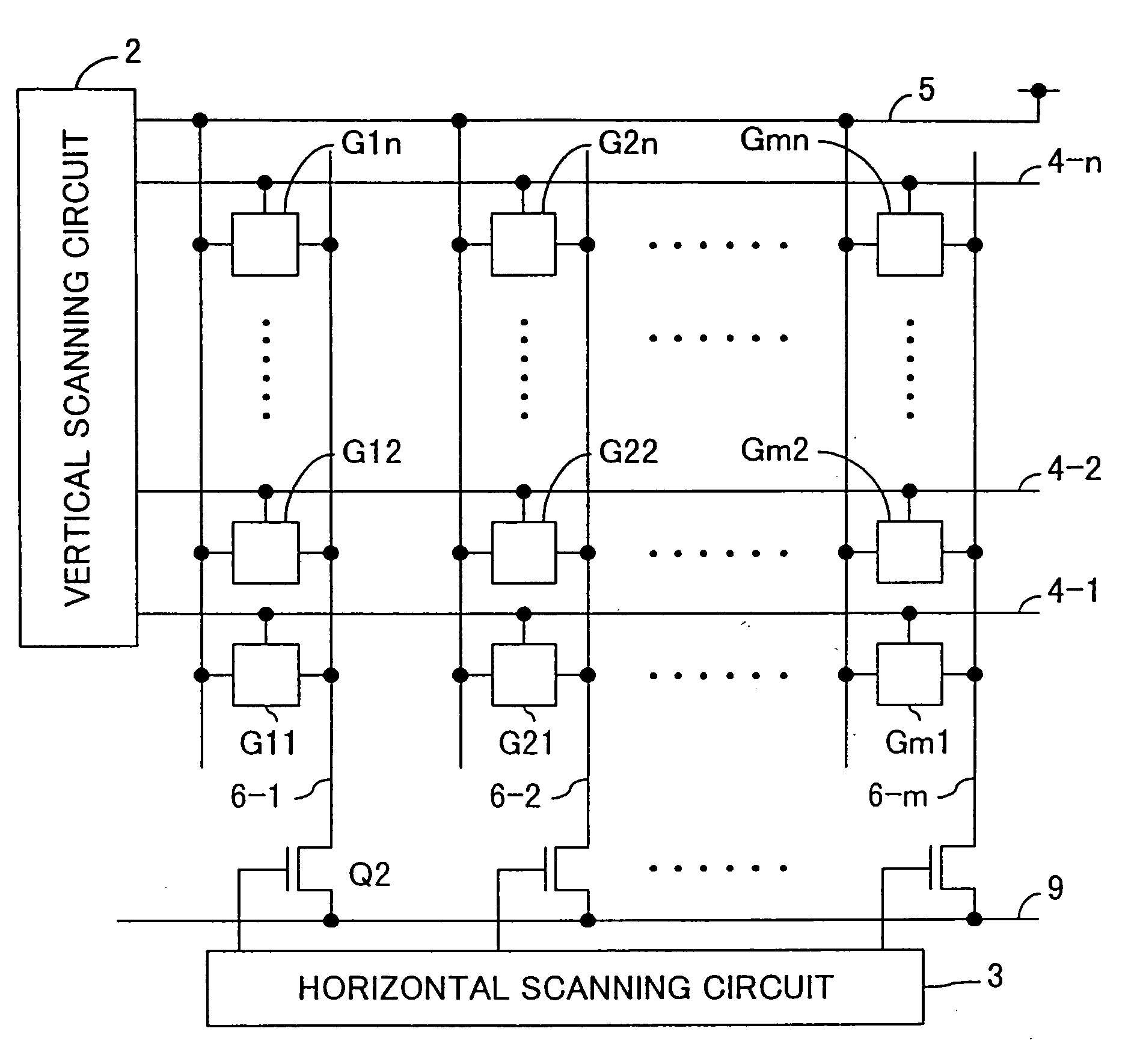
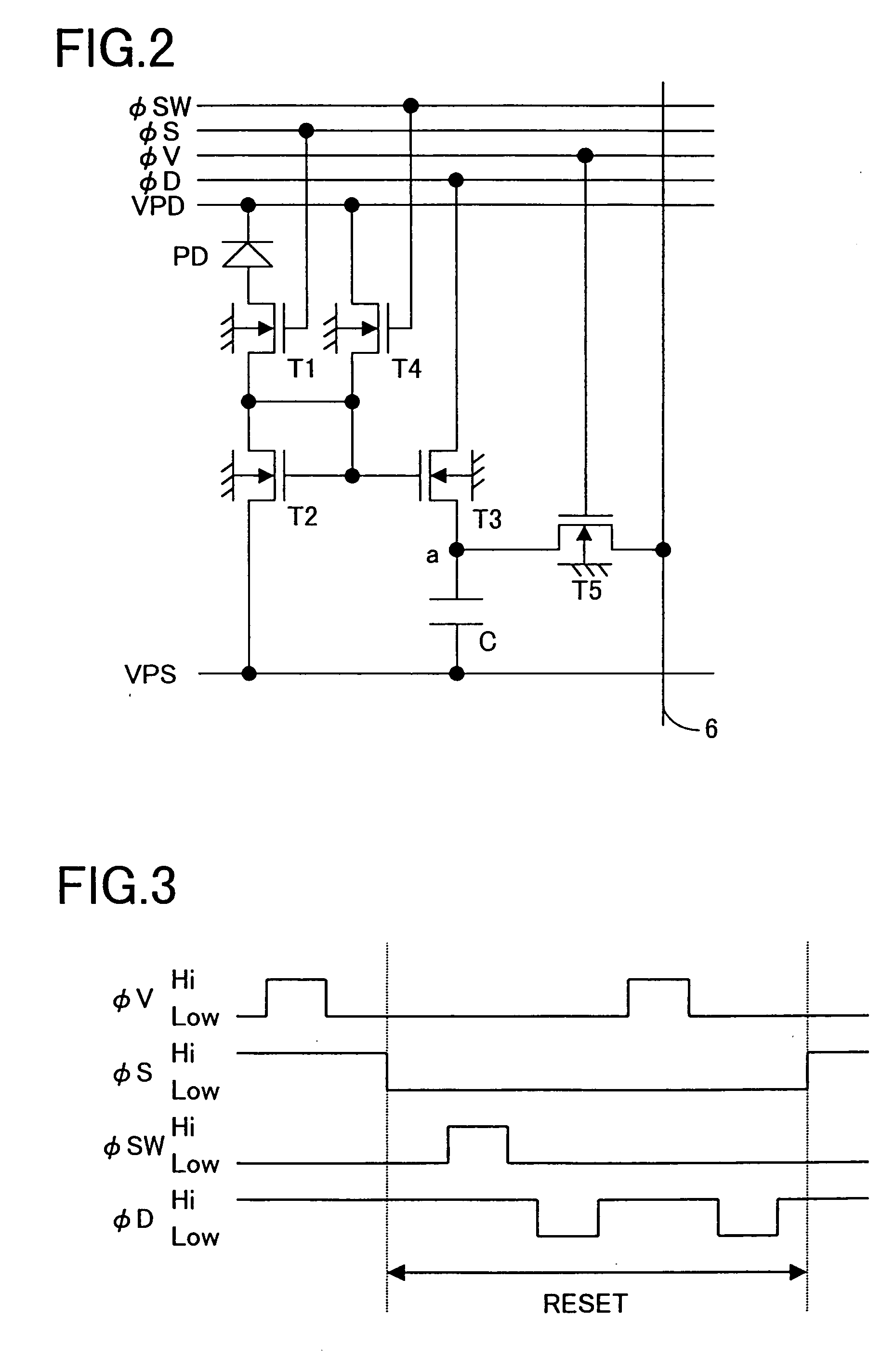
[0098] A first embodiment of the invention, which is applicable to each pixel of the first example of pixel configuration shown in FIG. 1, will be described below with reference to the drawings.

[0099] In FIG. 2, a pn photodiode PD constitutes a photosensor (photoelectric converter). The anode of this photodiode PD is connected to the drain of a MOS transistor T1. The source of this MOS transistor T1 is connected to the drain and gate of a MOS transistor T2, to the gate of a MOS transistor T3, and to the source of a MOS transistor T4. The source of the MOS transistor T3 is connected to the drain of a MOS transistor T5 for row selection. The source of this MOS transistor T5 is connected to an output signal line 6 (this output signal line 6 corresponds to the output signal lines 6-1, 6-2, . . . , 6-m in FIG. 1). The MOS transistors T1 to T5 are all N-channel MOS transistors with their back gates grounded.

[0100] A direct-current voltage VPD is applied to the cathode of the photodiode ...

second embodiment

[0117] A second embodiment of the invention, which is applicable to each pixel of the second example of pixel configuration shown in FIG. 5, will be described below with reference to the drawings. FIG. 7 is a circuit diagram showing the configuration of each pixel provided in the solid-state image-sensing device of this embodiment. In the following descriptions, such circuit elements, signal lines, and others as serve the same purposes as in the pixel shown in FIG. 2 are identified with the same reference numerals or symbols, and their detailed explanations will not be repeated.

[0118] As shown in FIG. 7, in this embodiment, as compared with the pixel shown in FIG. 2, a MOS transistor T6 having its gate connected to the node “a” so as to perform current amplification according to the voltage at the node “a”, a MOS transistor T5 for row selection having its drain connected to the source of the MOS transistor T6, and a MOS transistor T7 having its drain connected to the node “a” so as...

third embodiment

[0127] A third embodiment of the invention will be described below with reference to the drawings. FIG. 9 is a circuit diagram showing the configuration of each pixel provided in the solid-state image-sensing device of this embodiment. In the following descriptions, such circuit elements, signal lines, and others as serve the same purposes as in the pixel shown in FIG. 7 are identified with the same reference numerals or symbols, and their detailed explanations will not be repeated.

[0128] As shown in FIG. 9, in this embodiment, initialization of the capacitor C and the potential at the node “a” is achieved by feeding a signal φD to the drain of the MOS transistor T3. This makes it possible to omit the MOS transistor T7 found in the previous (second) embodiment. In other respects, the pixel of this embodiment is configured in the same manner as that of the second embodiment (FIG. 7). Here, as in the first embodiment (FIG. 2), in a period in which the signal φD is at a high level, th...


PUM


Abstract

In a solid-state image-sensing device, when an image sensing operation is performed in each pixel, a MOS transistor T1 is turned on and a MOS transistor T4 is turned off to make a MOS transistor T2 operate in a subthreshold region. When a reset operation is performed in each pixel, the MOS transistor T1 is turned off and the MOS transistor T4 is turned on to feed a constant voltage to the gate and drain of the MOS transistor T2. Then, the MOS transistor T4 is turned off, then the voltage at the node “a” is reset, and then a pulse signal φV is fed to a MOS transistor T5 to obtain an output. By using the thus obtained output as compensation data, variations in sensitivity among individual pixels are reduced.

Description

[0001] This application is based on Japanese Patent Applications Nos. 2000-28879, 2000-28946, and 2000-56029 filed respectively on Feb. 1, 2000, Feb. 1, 2000, and Feb. 28, 2000, the contents of which are hereby incorporated by reference. BACKGROUND OF THE INVENTION [0002] 1. Field of the Invention [0003] The present invention relates to a solid-state image-sensing device, and particularly to a solid-state image-sensing device having a plurality of pixels arranged therein. [0004] 2. Description of the Prior Art [0005] Solid-state image-sensing devices are not only small-sized, light-weight, and power-saving, but also free from image distortion, free from image burn-in, and resistant to unfavorable environmental conditions such as vibration and magnetic fields. Moreover, solid-state image-sensing devices can be manufactured by a process common or analogous to one used to manufacture LSIs (large-scale integrated circuits), and therefore they are reliable and fit for mass production. Fo...

Claims


Application Information

Patent Timeline
Patent Type & Authority Applications(United States)
IPC IPC(8): H04N5/335H04N5/355H04N5/3745
CPCH04N3/155H04N3/1568H04N5/35518H04N25/573
Inventor HAGIHARA, YOSHIO
Owner SONY SEMICON SOLUTIONS CORP
Why Eureka
Try Eureka