Wafer based camera module and method of manufacture

Active Publication Date: 2006-06-22
NANCHANG O FILM OPTICAL ELECTRONICS TECH CO LTD
View PDF28 Cites 116 Cited by
  • Summary
  • Abstract
  • Description
  • Claims
  • Application Information

AI Technical Summary

Benefits of technology

[0007] Accordingly, it is an object of the present invention to pr

Problems solved by technology

This arrangement requires a significant quantity of parts used in the attachment process.
It is also very labor intensive.
Additionally, the

Method used


Image

  • Wafer based camera module and method of manufacture
  • Wafer based camera module and method of manufacture
  • Wafer based camera module and method of manufacture

Examples


Embodiment Construction

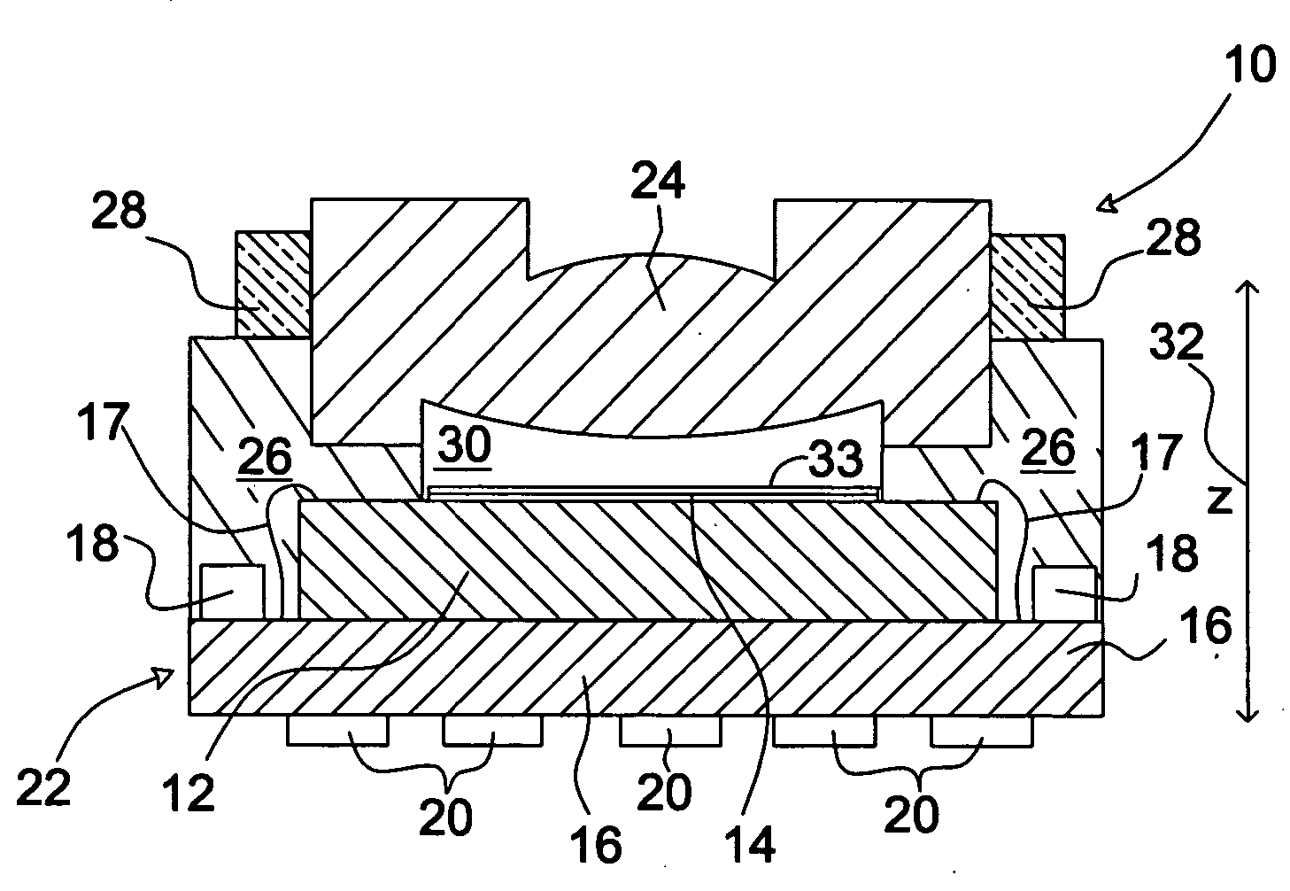
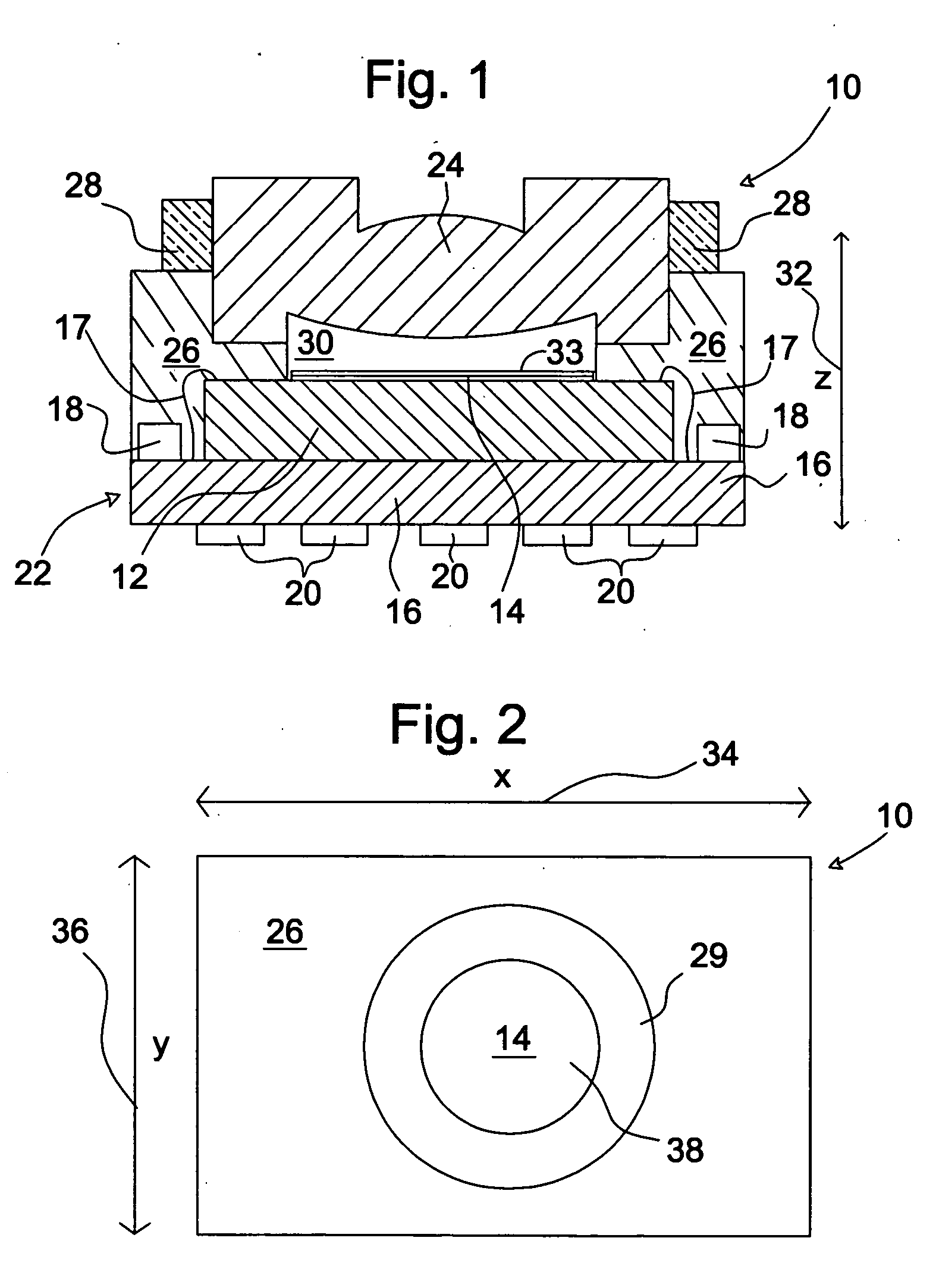
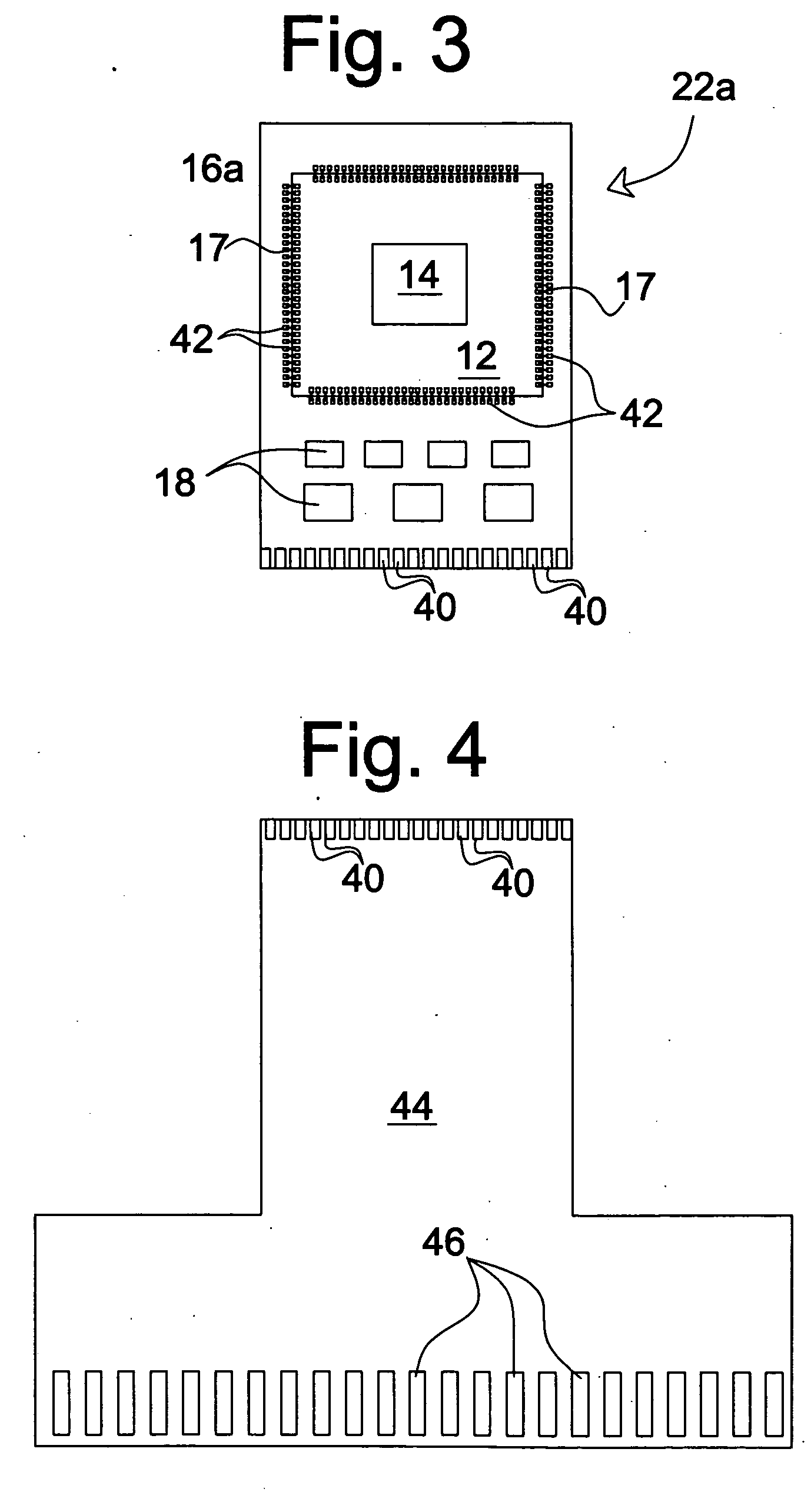
[0043] This invention is described in the following description with reference to the Figures, in which like reference numbers represent the same or similar elements. While this invention is described in terms of modes for achieving this invention's objectives, it will be appreciated by those skilled in the art that variations may be accomplished in view of these teachings without deviating from the spirit or scope of the present invention. The embodiments and variations of the invention described herein, and / or shown in the drawings, are presented by way of example only and are not limiting as to the scope of the invention. Unless otherwise specifically stated, individual aspects and components of the invention may be omitted or modified, or may have substituted therefore known equivalents, or as yet unknown substitutes such as may be developed in the future or such as may be found to be acceptable substitutes in the future. The invention may also be modified for a variety of appli...


PUM


Abstract

An integrated camera module (10, 10a) for capturing video images in very small digital cameras, cell phones, personal digital assistants, and the like. A lens assembly (24, 24a) is rigidly affixed in relation to a sensor array area (14) of a camera chip (12) by a molding (26). The molding (26) is formed on the camera chip (12), and optionally on a printed circuit board (16, 16a) on which the camera chip (12) is mounted. The lens assembly (24, 24a) is held in place in a recess (29) of the molding (26) by an adhesive (28). The molding (26) is formed such that a precise gap (30) exists between the lens assembly (24) and a sensor array area (14) of the camera chip (12). In a particular embodiment, lens holders (306, 506) are formed entirely on the camera chips (302, 502) before or after they are separated from one another.

Description

RELATED APPLICATIONS [0001] This application is a continuation-in-part of co-pending U.S. patent application Ser. No. 10 / 784,102, filed Feb. 20, 2004 by the same inventors, which is incorporated herein by reference in its entirety.BACKGROUND OF THE INVENTION [0002] 1. Field of the Invention [0003] The present invention relates generally to the field of digital camera devices, and more particularly to a novel combined array chip and lens apparatus. The predominant current application for the inventive integrated lens and chip assembly is in the production of low cost cameras, wherein the ability to produce high quality pictures without expensive or complicated camera assemblies is an important factor. [0004] 2. Description of the Background Art [0005] Very small digital camera modules, adapted for use in small inexpensive cameras, cell phones, hand held devices, and the like, are greatly in demand. In the prior art, such modules have included generally conventional integrated chip an...

Claims


Application Information

Patent Timeline
IPC IPC(8): H04N5/225H01L27/146H01L31/0232
CPCH01L27/14618H01L27/14625H01L27/14683H01L31/0203H01L31/0232H01L31/18H04N5/2253H04N5/2254H04N5/2257H01L2224/48091H01L31/02325H04N23/54H04N23/57H04N23/55H01L2924/00014
Inventor SHANGGUAN, DONGKAIKALE, VIDYADHAR SITARAMTAM, SAMUEL WAISING
Owner NANCHANG O FILM OPTICAL ELECTRONICS TECH CO LTD
Why Eureka
Try Eureka