Organic light emitting display device and method of fabricating the same

Active Publication Date: 2006-07-06
SAMSUNG DISPLAY CO LTD
View PDF9 Cites 40 Cited by
  • Summary
  • Abstract
  • Description
  • Claims
  • Application Information

AI Technical Summary

Problems solved by technology

However, since the liquid crystal display device is not a self-emitting device and instead is a light receiving device, it has a limitation in brightness, contrast, viewing angle, large-sized display, and so on.
By contrast, the PDP is a self-emitting device, but it is heavier than the other flat panel display devices and has high power consumption, and its manufacturing method is complicated.
However, the broad width of the conventional common power supply bus line and cathode bus line makes it difficult to increase an area of the light emitting portion.

Method used


Image

  • Organic light emitting display device and method of fabricating the same
  • Organic light emitting display device and method of fabricating the same
  • Organic light emitting display device and method of fabricating the same

Examples


Embodiment Construction

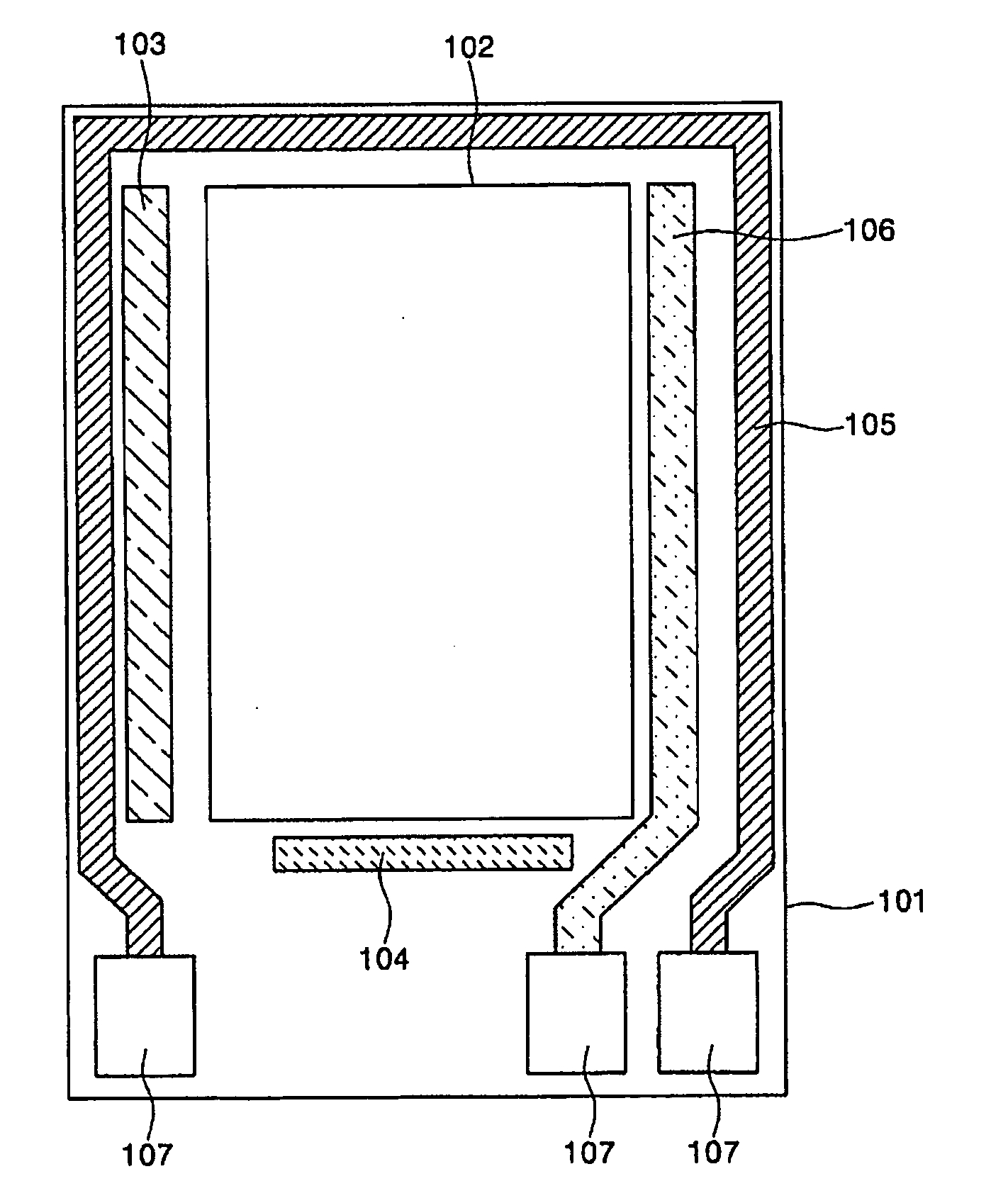
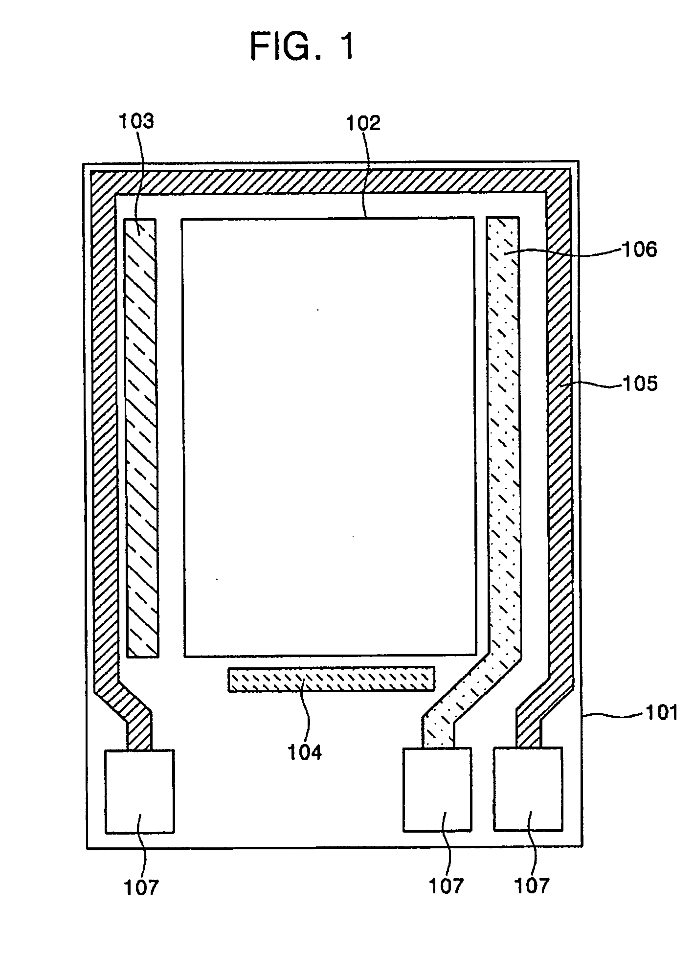
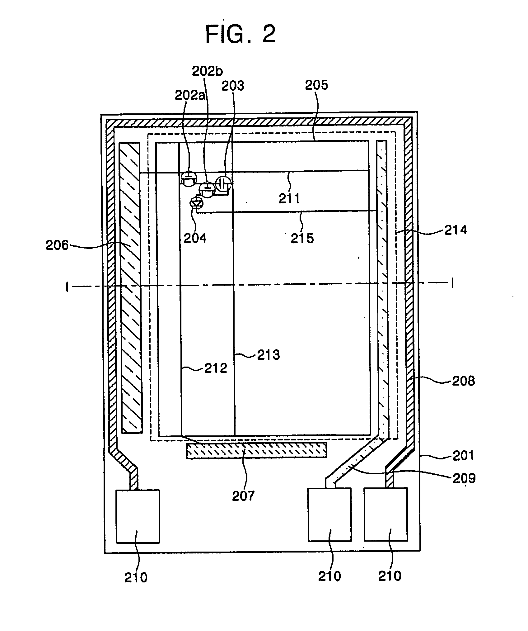
[0018] In the following detailed description, certain exemplary embodiments of the present invention are shown and described, by way of illustration. As those skilled in the art would recognize, the described exemplary embodiments may be modified in various ways, all without departing from the spirit or scope of the present invention. Accordingly, the drawings and description are to be regarded as illustrative in nature, rather than restrictive. There may be parts shown in the drawings, or parts not shown in the drawings, that are not discussed in the specification as they are not essential to a complete understanding of the invention. In the drawings, the thickness of layers and regions are exaggerated for clarity. Like reference numerals designate like elements throughout the specification. In addition, when a first element is on a second element, the first element may not only be directly on the second element but may also be indirectly on the second element via a third element. ...


PUM


Abstract

An OLED display device and a method of fabricating the same. The OLED display device has at least one of a common power bus line or a cathode bus line formed at a peripheral portion of the OLED display device. By forming a lower line when a gate electrode of a thin film transistor is formed, and forming an upper line connected to the lower line through a contact hole when source and drain electrodes of the thin film transistor are formed, a dual structure of lower and upper lines is formed. As such, the OLED display device can reduce the width of interconnections without a high voltage drop to thereby increase an emission area of a light emitting portion of the OLED display device.

Description

CROSS-REFERENCE TO RELATED APPLICATION [0001] This application claims priority to and the benefit of Korean Patent Application No. 10-2005-0000992, filed Jan. 5, 2005, the entire content of which is incorporated herein by reference. BACKGROUND OF THE INVENTION [0002] 1. Field of the Invention [0003] The present invention relates to an organic light emitting diode (OLED) display device and a method of fabricating the same and, more particularly, to an OLED display device and a method of fabricating the same having a dual structure of lower and upper lines connected through a contact hole to form a common power bus line and / or a cathode bus line. [0004] 2. Description of the Related Art [0005] Recently, in order to reduce the heavyweight and large volume of a conventional display device such as a cathode ray tube, attentions have been directed to flat panel display devices such as a liquid crystal display device, an OLED display device, a plasma display panel, and so on. [0006] Howeve...

Claims


Application Information

Patent Timeline
IPC IPC(8): H01J1/62
CPCH01L27/124H01L27/3276H10K59/131H05B33/26H05B33/10
Inventor LEE, SU-MI
Owner SAMSUNG DISPLAY CO LTD
Why Eureka
Try Eureka