
Semiconductor device

a technology of semiconductor devices and semiconductors, applied in the direction of semiconductor devices, basic electric elements, electrical equipment, etc., can solve the problems that the semiconductor device cannot be used, and achieve the effect of simplifying the structure of the section, miniaturizing the semiconductor device, and easy miniaturization

Active Publication Date: 2006-07-13
SHINDENGEN ELECTRIC MFG CO LTD
View PDF2 Cites 4 Cited by
  • Summary
  • Abstract
  • Description
  • Claims
  • Application Information

AI Technical Summary

Benefits of technology

[0010] Accordingly, since the plurality of conductive areas of the second conductive type are formed in the direction across the grooves, almost all sections surrounded by these conductive areas and the grooves can be assigned as the fourth conductive layer. In other words, it is possible to simplify the structure of a section interposed between the grooves, so that the miniaturization of this section becomes easy.
[0014] According to the present invention, since the plurality of conductive areas of the second conductive type are formed across the grooves, so that it is possible to assign almost all sections surrounded by these conductive areas and the grooves as a single conductive layer. Therefore, the structure of this section is simplified, and hence the miniaturization of the semiconductor device becomes easy. Also there is the advantage that the introduction of expensive semiconductor production equipment is unnecessary for miniaturizing the semiconductor device.
[0015] The first grooves are formed across the second grooves, and the different conductive layers or areas are exposed from the surfaces of these grooves. Thus, it is possible to assign almost all sections surrounded by the first grooves and the second grooves as a single conductive layer. Therefore, the structure of this section is simplified, and hence the miniaturization of the semiconductor device becomes easy.

Problems solved by technology

Such a semiconductor device cannot be used since it exhibits electric characteristics, which a designer does not plan.
Therefore, this problem related to the width of mesa “W” has become a significant factor preventing the miniaturization of such semiconductor devices.

Method used


Image

  • Semiconductor device
  • Semiconductor device
  • Semiconductor device

Examples


Embodiment Construction

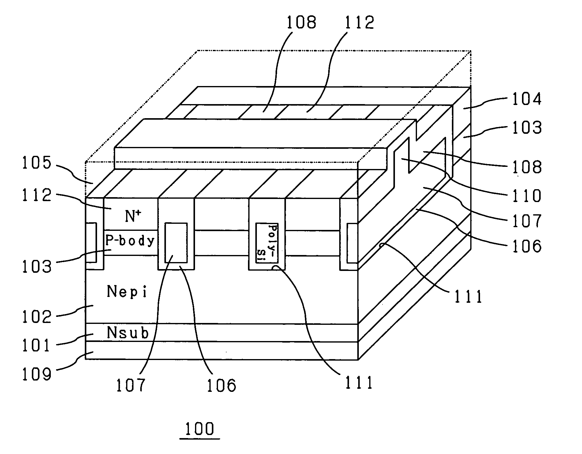
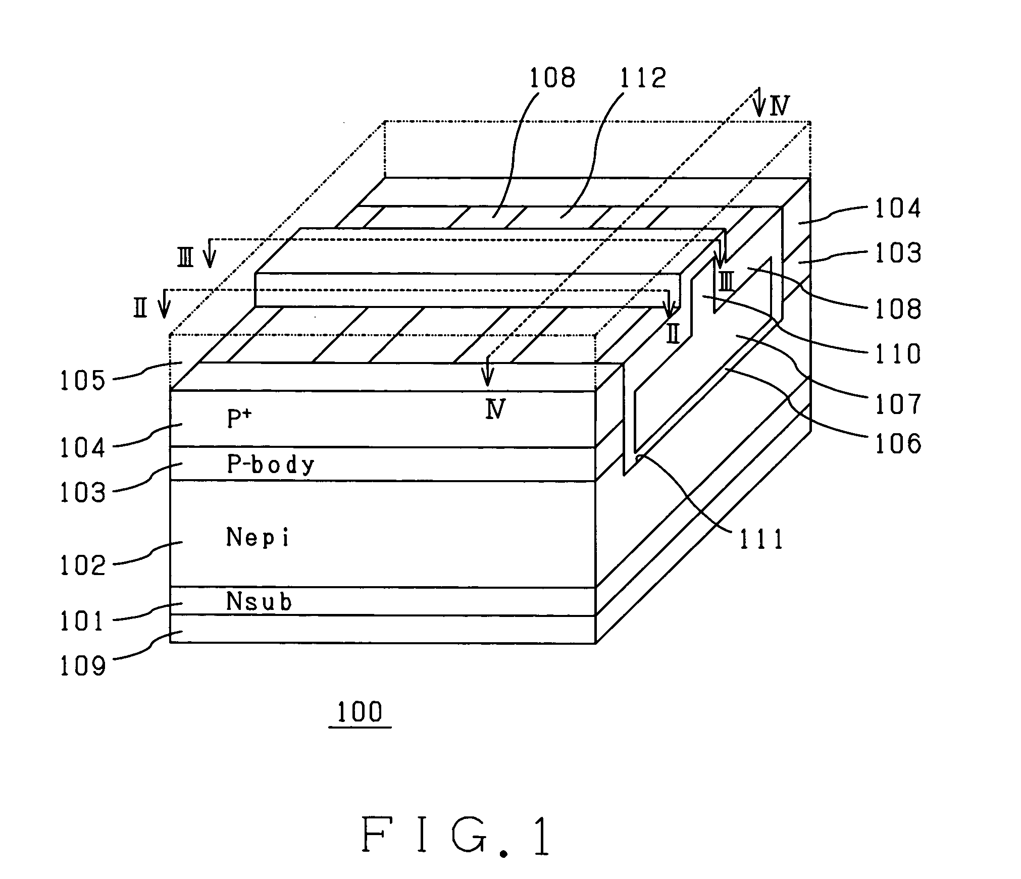
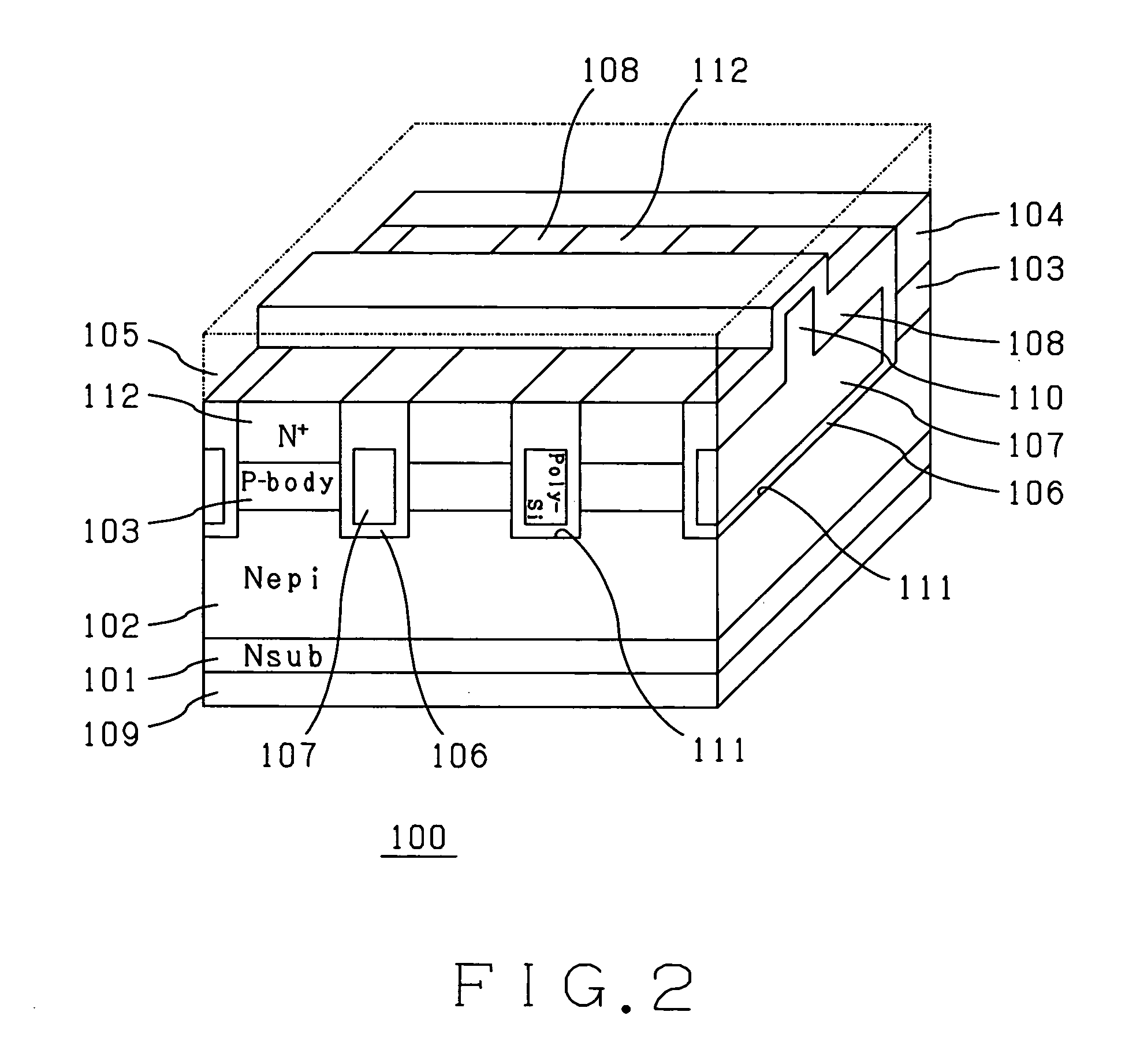
[0027] One feature of the present invention is that a source area and a P type body layer are disposed in a mesa section sandwiched between gate trenches, while a P type diffusion area is disposed in a section other than the mesa section. Another feature of the present invention is that a connection member is formed so as to intersect with the gate trenches, and gate electrode films are connected to each other by connecting the gate electrode films and upper gate electrode films, which are disposed under the connection member, to the connection member. Still another feather of the present invention is that a P type area, for easing an electric field, is formed so as to cover the corners of the gate trenches. This is for the purpose of easing electric field intensity in the vicinity of the corners of the gate trenches. The present invention will be hereinafter described in detail on the basis of illustrated embodiments.

[0028]FIG. 1 is a perspective view of a semiconductor device acc...


PUM


Abstract

In a semiconductor device in which gate trenches and source trenches are formed, when the semiconductor device is flatly viewed, N+ type source areas are formed in parallel with the gate trenches to ease the miniaturization of the semiconductor device. P+ type diffusion areas are separately formed in a direction orthogonal to the N+ type source areas and the gate trenches. Thus, the N+ type source areas and a P type body layer are formed in a laminated state, but the P+ type diffusion areas are not laminated. Therefore, the structure of a mesa section is extremely simple. Furthermore, gate electrode films are connected to one another by a connection member. Thus, the semiconductor device has such a structure as to easily secure electric connection to each gate electrode film from outside. According to the foregoing structure, it is possible to extremely ease the miniaturization of the semiconductor device.

Description

FIELD OF THE INVENTION [0001] The present invention relates to a semiconductor device, and in particular, to a semiconductor device having the structure of a power MOSFET that is mainly used in a power supply circuit and the like. BACKGROUND OF THE APPLICATION [0002] A semiconductor device having the structure of a power MOSFET, in which gate trenches and source trenches are formed, has been widely applied in recent years to various power supplies such as DC-DC converters. FIG. 11 shows an example of such a semiconductor device. FIG. 11 is a sectional view showing an example of a semiconductor device according to conventional technology. In FIG. 11, a semiconductor device 300 comprises an N+ type drain layer 301, an N− type drift layer 302, a P type body layer 303, P+ type diffusion areas 304, a source electrode film 305, gate insulating films 306, gate electrode films 307, a drain electrode film 309, gate trenches 311, N+ type source areas 312, source trenches 313, an insulating fi...

Claims


Application Information

Patent Timeline
Patent Type & Authority Applications(United States)
IPC IPC(8): H01L31/072
CPCH01L29/1095H01L29/41766H01L29/4236H01L29/7813
Inventor TAKEMORI, TOSHIYUKISASAOKA, FUMINORIWATANABE, YUJI
Owner SHINDENGEN ELECTRIC MFG CO LTD
Learn More