Solid State Image Pickup Apparatus, Camera and Driving Method of Solid State Image Pickup Apparatus
a pickup apparatus and solid state technology, applied in the direction of instruments, television systems, code conversion, etc., can solve the problems of excessive restriction of the operation speed of the cmos area sensor, and difficulty in suitably picking up a moving imag
- Summary
- Abstract
- Description
- Claims
- Application Information
AI Technical Summary
Problems solved by technology
Method used
Image
Examples
first embodiment
[0027] Next, a first embodiment of the present invention is described with reference to the attached drawings.
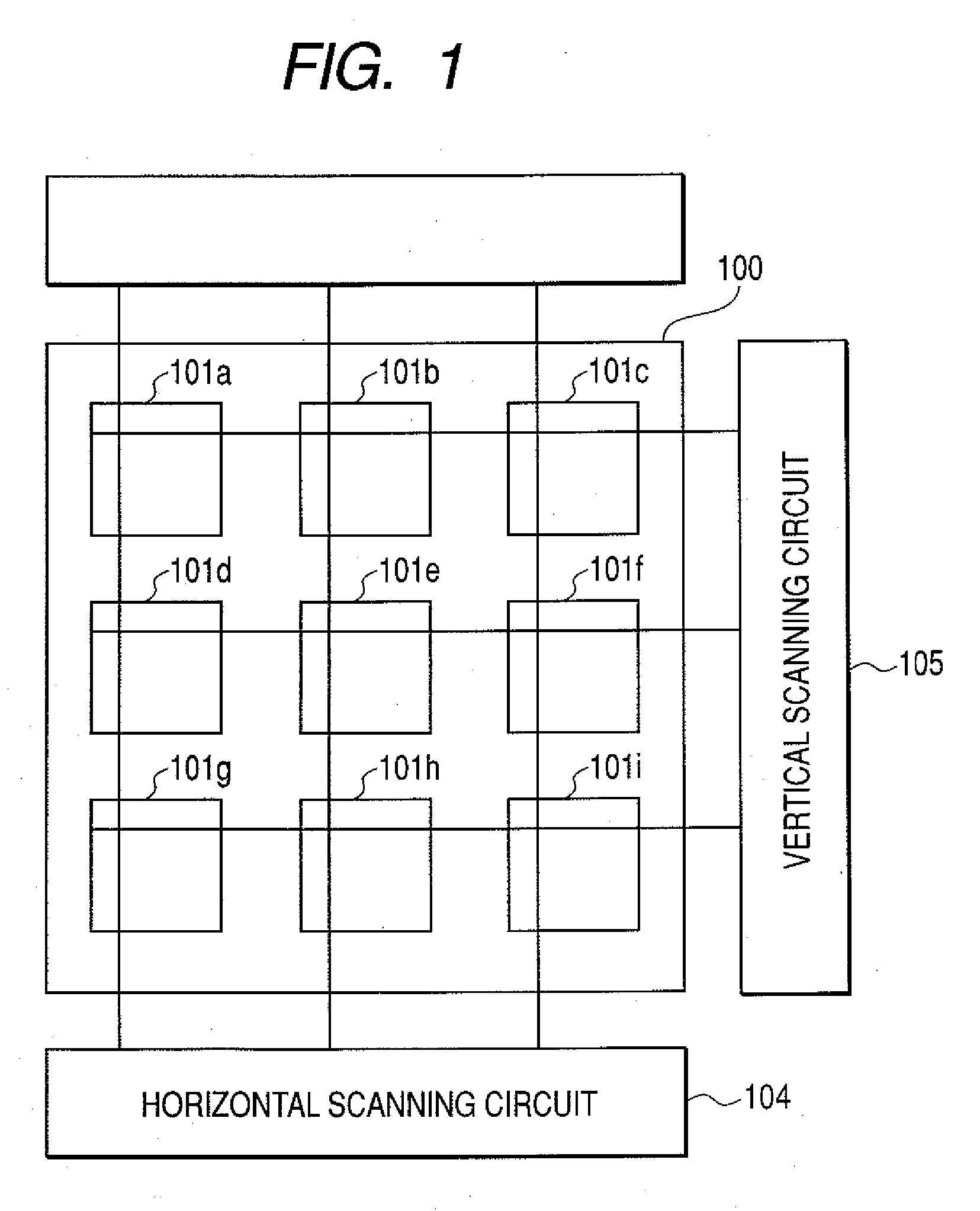
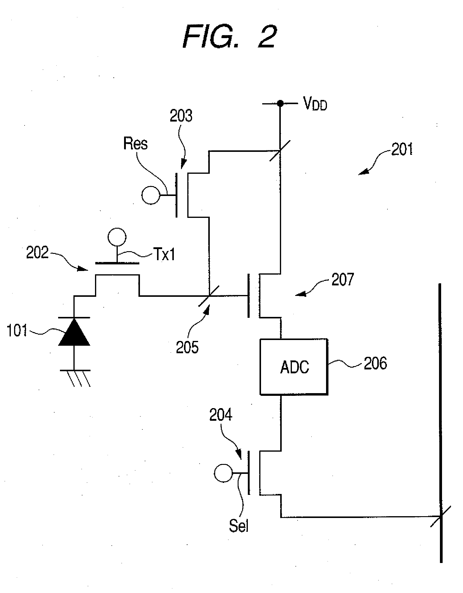
[0028]FIG. 1 is a diagram showing an example of the schematic configuration of a solid state image pickup apparatus of the present embodiment. FIG. 2 is a diagram showing an example of an equivalent circuit of a CMOS sensor unit 101.
[0029] In FIG. 1, a pixel area 100 is composed of a plurality of CMOS sensor units (pixels) 101a to 101i arranged in a two-dimensional matrix of three rows by three columns, each composed of a photoelectric conversion unit (for example, a photodiode) 201, transistors 202, 203, 204 and 207 and an AD converter 206.
[0030] Incidentally, although the plurality of CMOS sensor units (pixels) 101a to 101i is arranged in the two-dimensional matrix of three rows by three columns in FIG. 1, the number of arrangement of the CMOS sensor unit (pixel) 101 is not limited to this arrangement. For example, the plurality of CMOS sensor units (pixels) 101 may be ...
second embodiment
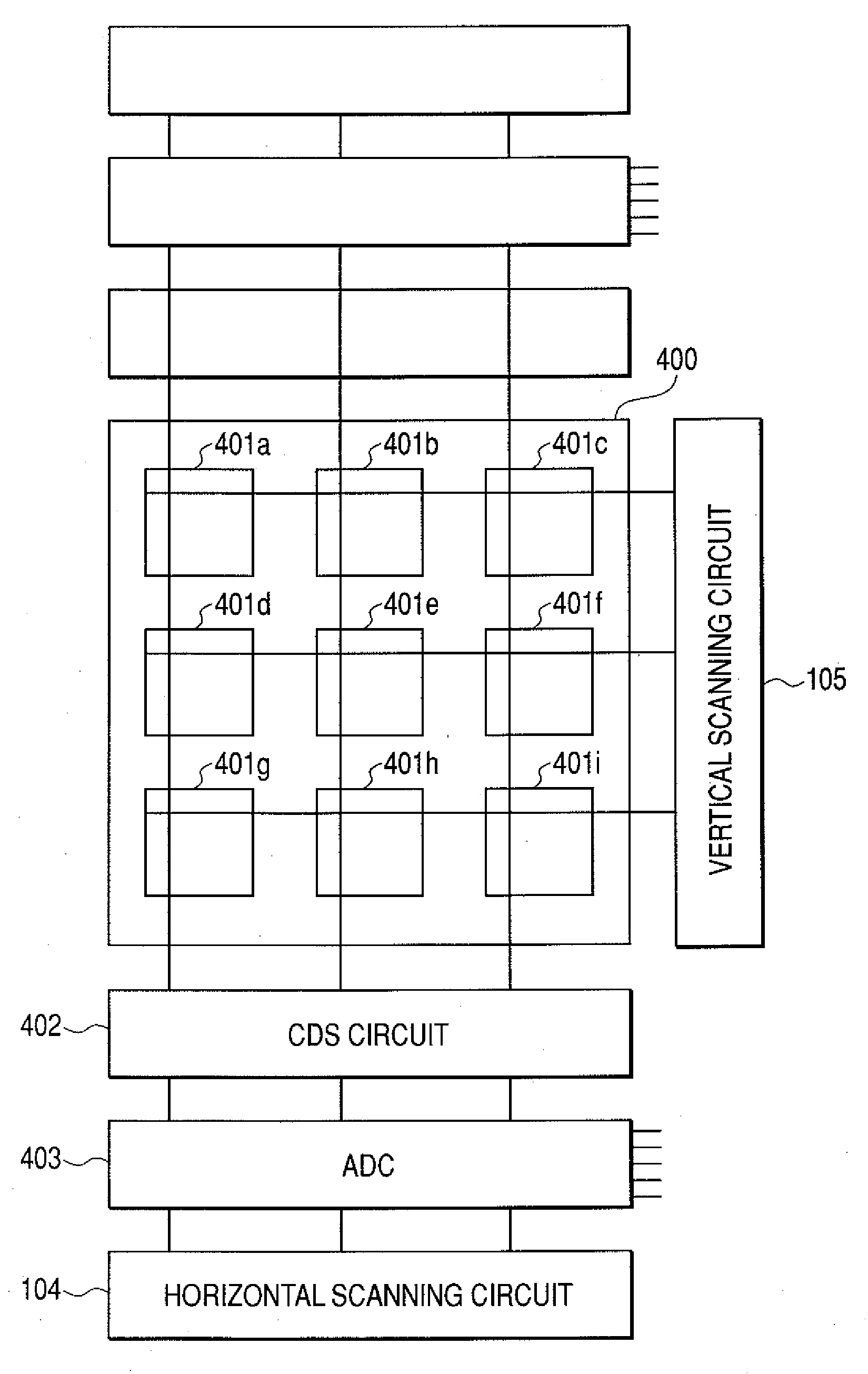
[0057] Next, a second embodiment of the present invention is described. In the first embodiment described above, the AD converter 206 is provided to each pixel, and an analog signal is converted into a digital signal in each pixel. On the other hand, in the present embodiment, an analog signal is converted into a digital signal by each column. In this manner, because the present embodiment differs from the first embodiment only in the method of converting an analog signal into a digital signal, in the following descriptions, by denoting the same portions as those of the first embodiment by the same reference marks as those shown in FIGS. 1 to 3, and the like, the detailed descriptions of the same portions are omitted.
[0058]FIG. 4 is a diagram showing an example of the schematic configuration of a solid state image pickup apparatus of the present embodiment.
[0059] In FIG. 4, a pixel area 400 is the same one as the pixel area 100 of the first embodiment excluding the AD converters 2...
third embodiment
[0073] Next, a third embodiment of the present invention is described. In the present embodiment, a multi integrating type AD converter is used as the AD converter for each column. The present embodiment differs from the second embodiment only in that the configuration of the AD converter is different from that of the second embodiment. Accordingly, by denoting the same portions as those of the first and the second embodiments with the same reference marks as those shown in FIGS. 1 to 6, or by performing the similar mediums, the detailed descriptions of the same portions are omitted.
[0074]FIG. 7 is a diagram showing an example of the circuit configuration of the AD converter of the present embodiment. Incidentally, the comparators 501a to 501c and so forth are basically the same circuits as those of the second embodiment except for having a plurality of kinds of memory units through switches. Accordingly, in FIG. 7, a part of the circuits of the AD converters is omitted, and the de...
PUM
 Abstract
Description
Claims
Application Information


