Automated sub-field blading for leveling optimization in lithography exposure tool

Inactive Publication Date: 2006-07-20
IBM CORP
View PDF6 Cites 24 Cited by
  • Summary
  • Abstract
  • Description
  • Claims
  • Application Information

AI Technical Summary

Benefits of technology

[0010] Bearing in mind the problems and deficiencies of the prior art, it is therefore an object of the present invention to provide a s

Problems solved by technology

Unanticipated topography variation on the substrate has become a significant problem for many next generation lithography processes using high numerical aperture (NA) imaging.
The trend of increasing NA allows increased resolution but this comes at the expense of process DOF.
In the case where the pre-scan detects significant changes in step height across the exposure slit, there is limited ability to compensate.
Since image focus cannot be varied across the slit, the tool must attempt to balance out this error using linear wafer stage movements.
This is in fact the limit of today's exposure tools.
In fact, with significant step heights, many areas across this slit still see significant deviation from best focus.
When the process does not have adequate DOF to support these deviati

Method used


Image

  • Automated sub-field blading for leveling optimization in lithography exposure tool
  • Automated sub-field blading for leveling optimization in lithography exposure tool
  • Automated sub-field blading for leveling optimization in lithography exposure tool

Examples


Embodiment Construction

)

[0040] In describing the preferred embodiment of the present invention, reference will be made herein to FIGS. 1-6 of the drawings in which like numerals refer to like features of the invention.

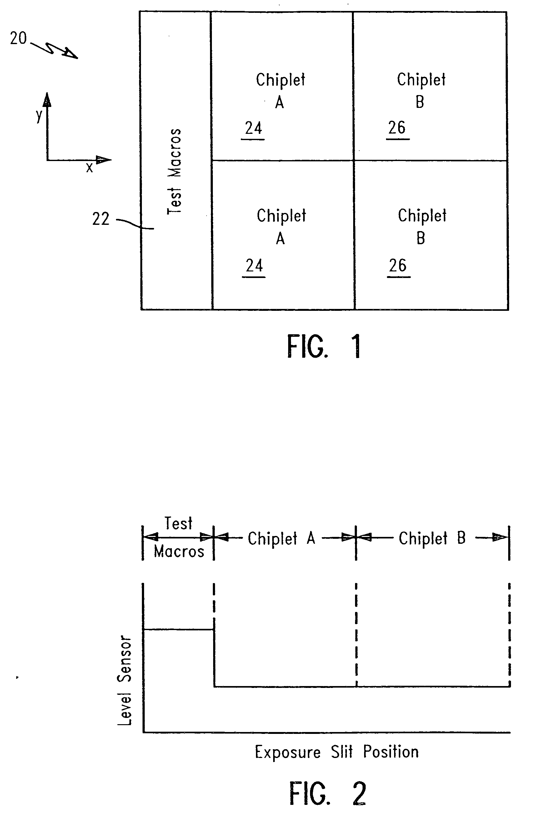
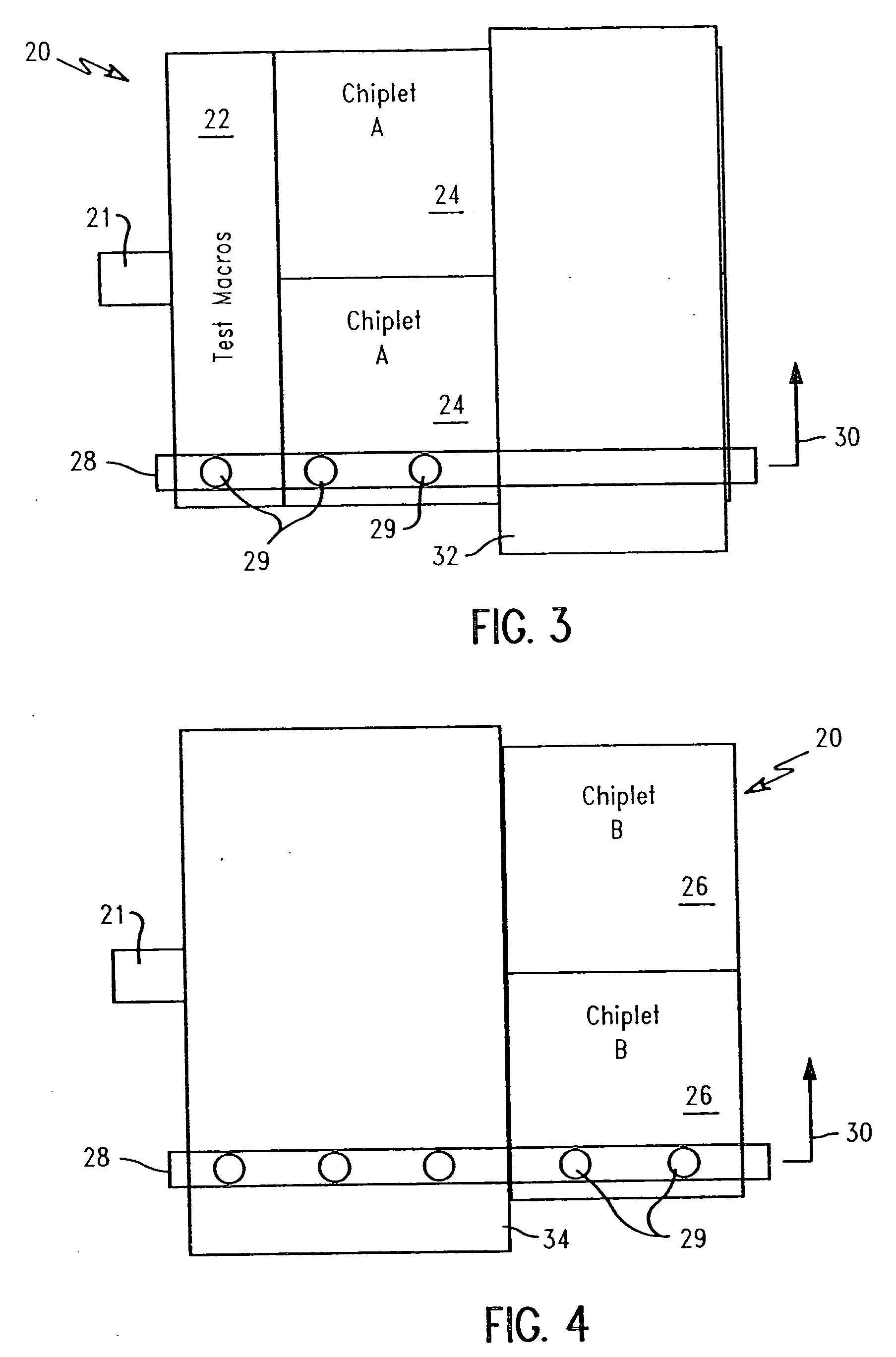
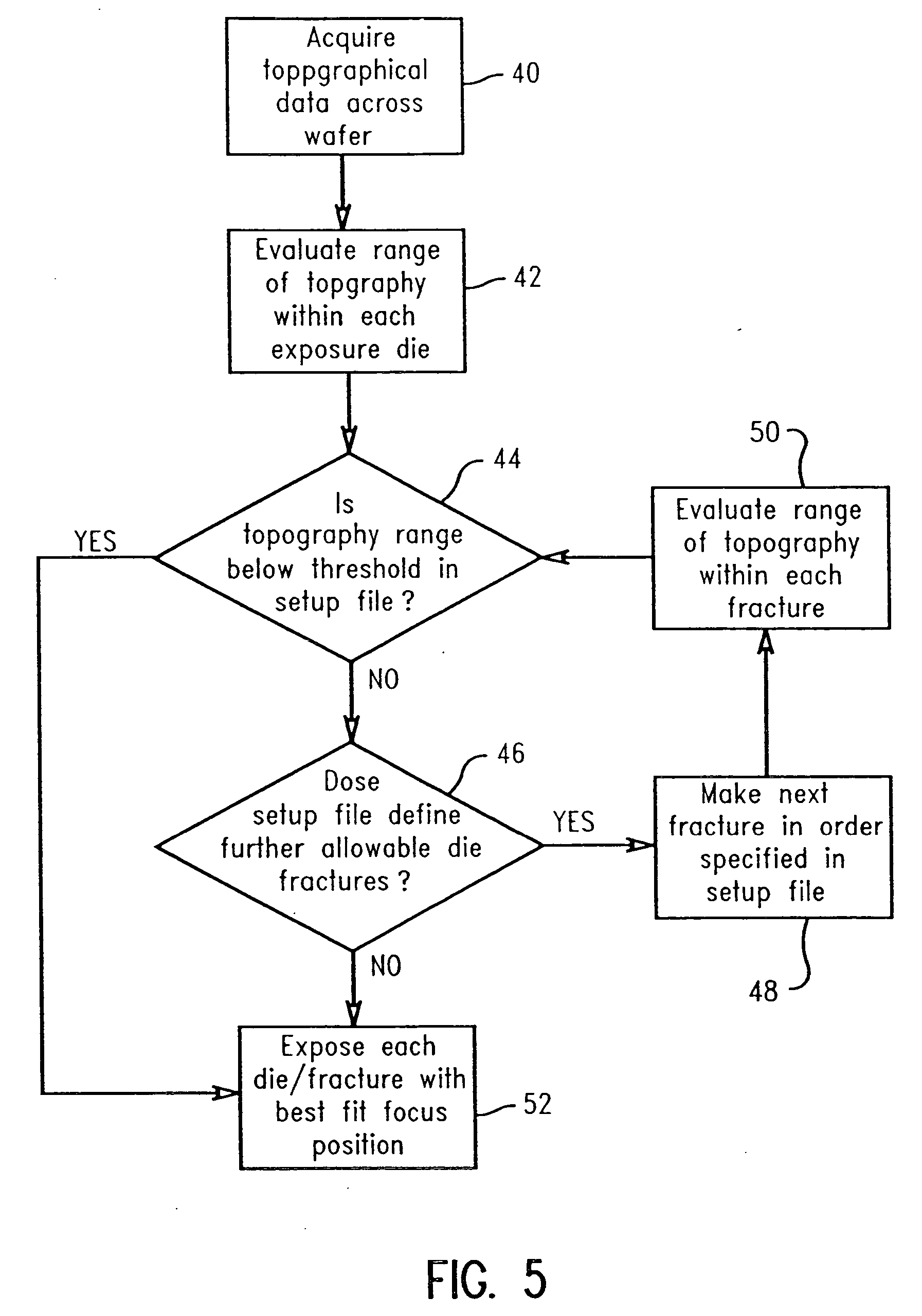
[0041] The present invention divides or fractures portions of the wafer, also know as chiplets, into different scanning regions based on topographical data, and then incorporates potential chiplet fracturing in the reticle design and provides the exposure system with detailed information regarding these potential fracture points. With this information, the exposure tool can monitor and compensate the step height differences induced by variations in different areas of the wafer, e.g., from one customer part to another, or between test macros and product chips. In cases where significant topography variation is detected and exceeds the predetermined process DOF, the method of the present invention breaks the die down based on the predetermined fracture points and uses the exposure tool scanne...


PUM


Abstract

A method of exposing images on a wafer having varying topography during lithographic production of microelectronic devices. The method initially includes determining topography of a wafer, dividing the wafer into two or more separate regions based on the wafer topography, and determining desired focus distance for exposing a desired image on each of the separate regions of the wafer. The method then includes exposing a desired image on one of the regions of the wafer at the desired focus distance while blocking remaining regions and exposing a desired image on another of the regions of the wafer at the desired focus distance while blocking remaining regions. The desired focus distance may be different for each of the separate wafer regions.

Description

BACKGROUND OF THE INVENTION [0001] 1. Field of the Invention [0002] This invention relates to lithographic production of microelectronic devices and, in particular, to the lithographic exposure tools utilized therein to expose circuit patterns and other images on the surface of the wafer used to produce the microelectronic device. [0003] 2. Description of Related Art [0004] Lithographic processing generally involves exposing a desired pattern onto a resist layer on a wafer substrate layer using a step-and-scan exposure tool, developing the resist layer to remove the portions exposed (or not exposed), and then further processing the wafer, for example, by etching the underlying layer or depositing additional material, using the developed resist layer. Lithographic imaging is highly dependent on substrate uniformity to create an accurate circuit pattern on the surface of an individual wafer layer to be lithographically processed. A lithographic process can tolerate a small range of to...

Claims


Application Information

Patent Timeline
IPC IPC(8): G03F7/20
CPCG03F7/70466
Inventor BRODSKY, COLIN J.BUKOFSKY, SCOTT J.HOLMES, STEVEN J.
Owner IBM CORP
Why Eureka
Try Eureka