

Electron beam exposure apparatus
a technology of exposure apparatus and electron beam, which is applied in the field of exposure apparatus, can solve the problems of increasing the load of the mounting b>5/b> due to an increase in the mass of the sample chamber b>3/b>, increasing the operation time, and increasing so as to reduce the measurement error of the stage position and achieve high-precision exposure
- Summary
- Abstract
- Description
- Claims
- Application Information
AI Technical Summary
Benefits of technology
Problems solved by technology
Method used
Image

Examples
first embodiment
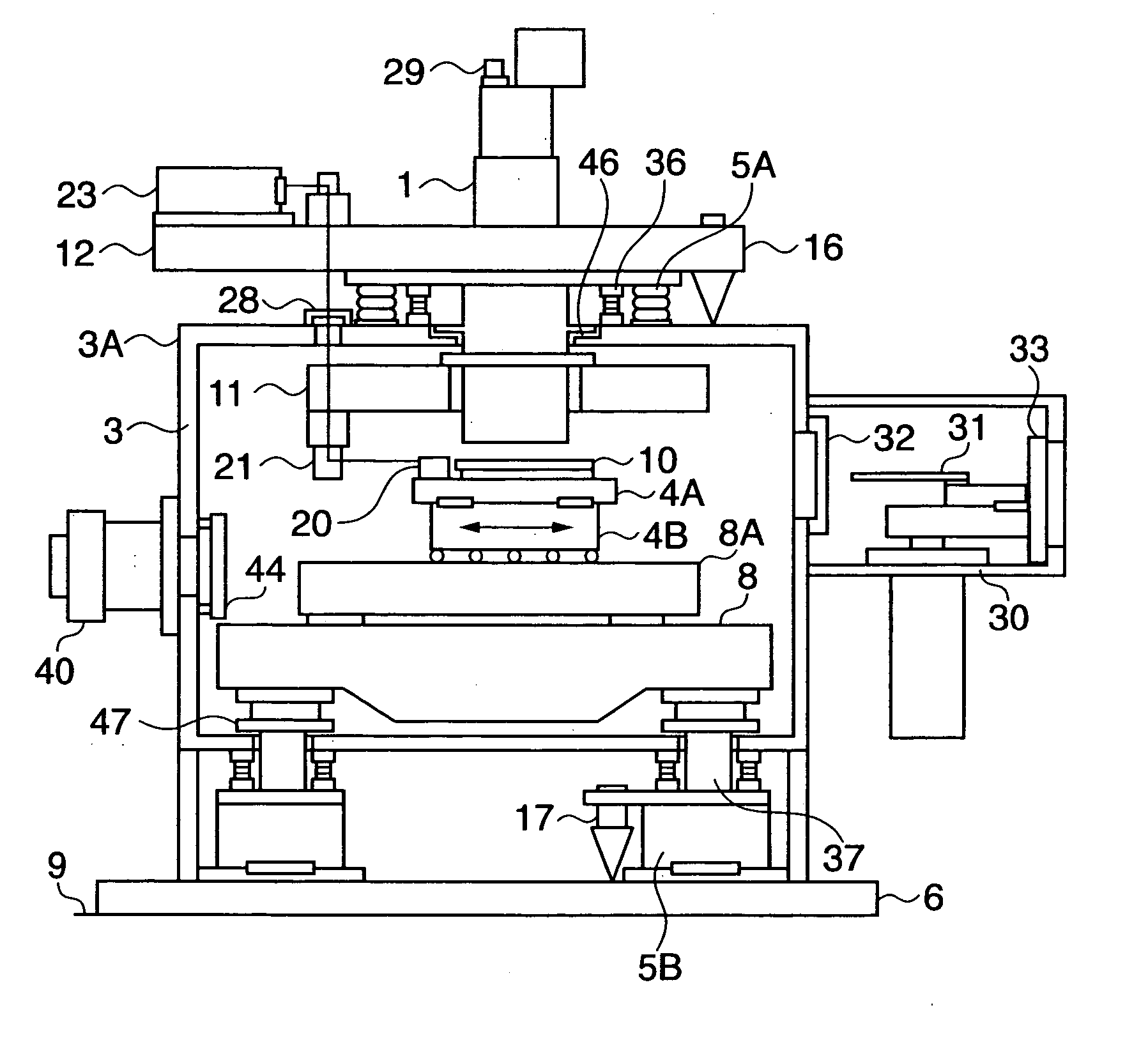
[0059]FIG. 1 is a diagram showing a brief construction of an electron beam exposure apparatus according to the first embodiment of the present invention. In FIG. 1, a sample chamber 3 which is a vacuum vessel is arranged on a base 6. The sample chamber 3, arranged on the base 6, separates the internal space for processing a sample from the external space by partitions (enclosure members) including, e.g., the bottom partition, side partition, and upper partition 3A. The sample chamber 3 can receive a wafer or the like as a sample of an exposure target. The partitions are provided with magnetic shields made of a magnetic material, so that the geomagnetism is attenuated in the internal space. Provided on the side partition is a vacuum pump opening, where a vacuum pump 40 is arranged for exhausting the sample chamber. On the vacuum pump opening, a magnetic shield 44 is arranged for attenuating the geomagnetism intruding inside the sample chamber 3 from the opening. Because of these magn...
second embodiment
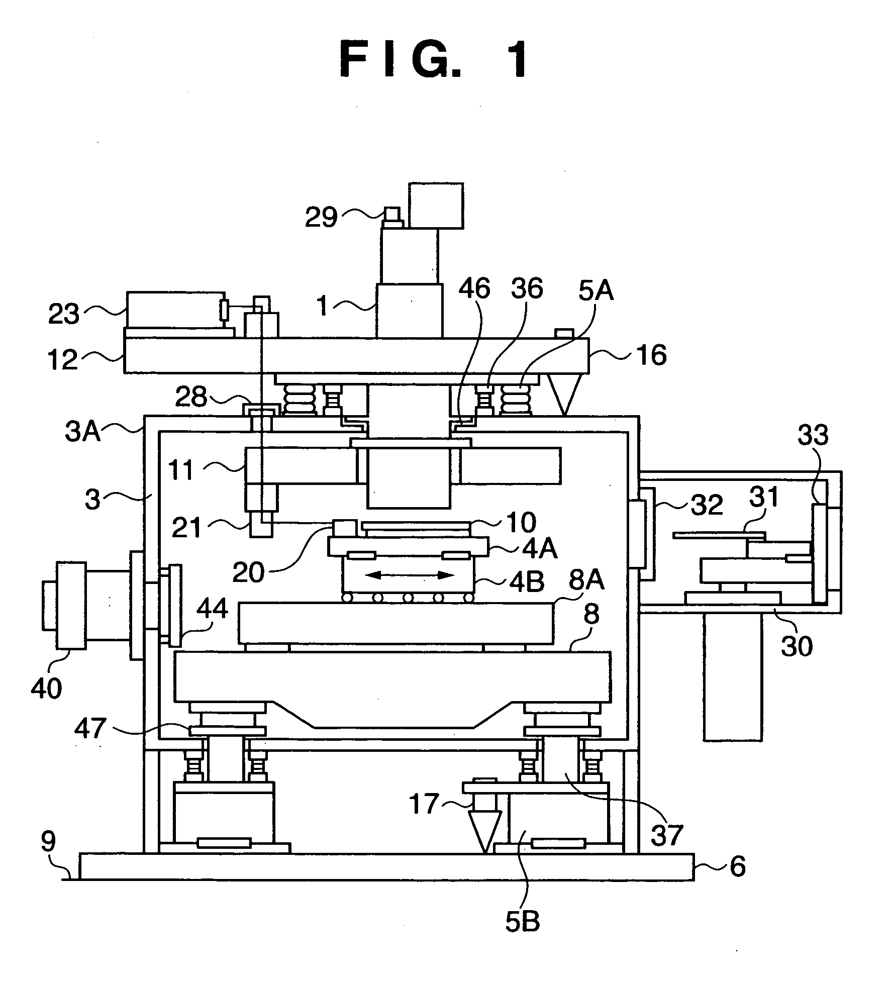
[0083]FIG. 2 is a diagram showing a brief construction of an electron beam exposure apparatus according to the second embodiment of the present invention. In FIG. 2, a sample chamber 3 which is a vacuum vessel is arranged on a base 6. The sample chamber 3, arranged on the base 6 through the second mounting 5B, separates the internal space for processing a sample from the external space by partitions (enclosure members) including, e.g., the bottom partition, side partition, and upper partition3A. The partitions are provided with magnetic shields made of a magnetic material, so that the geomagnetism is attenuated in the internal space. Provided on the side partition is a vacuum pump opening, where a vacuum pump 40 is arranged for exhausting the sample chamber. On the vacuum pump opening, a magnetic shield 44 is arranged for attenuating the geomagnetism intruding inside the sample chamber 3 from the opening. Because of these magnetic shields, the interior of the sample chamber 3 is kep...
third embodiment
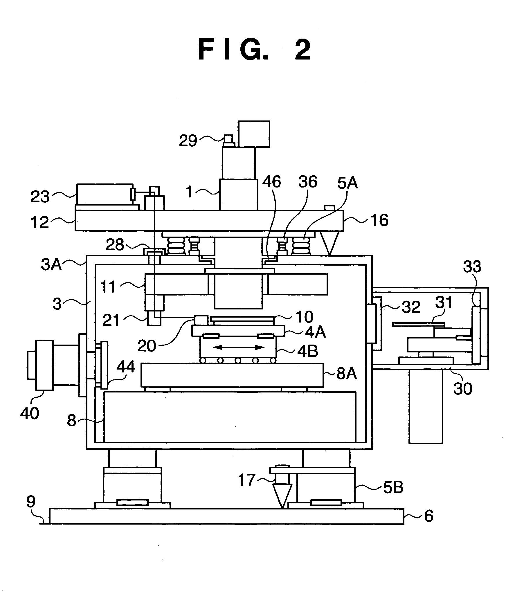
[0105]FIG. 3 is a diagram showing a brief construction of an electron beam exposure apparatus according to the third embodiment of the present invention. In FIG. 3, the sample chamber 3, the column 1, the stages 26 and 27 have constructions according to the first embodiment. A reaction force receiver of the third embodiment, which is added to the construction of the first embodiment, is described. By virtue of providing the reaction force receiver, it is possible to reduce oscillation and vibration on the entire portion above the second mounting 5B, which is generated by the reaction force caused by counteraction of acceleration or deceleration of the conveying stage 26. Furthermore, since the relative position between the column 1 and the movable mirror 20 (consequently the relative position between the column 1 and the sample stage 4A (moreover the sample)) is servo-controlled, it is possible to reduce vibration of the column 1, the first reference structural member 11, and the se...
PUM
 Abstract
Description
Claims
Application Information