Semiconductor manufacturing apparatus

a manufacturing apparatus and semiconductor technology, applied in the direction of manufacturing tools, metal-working machine components, large fixed members, etc., can solve the problems of difficult to correct the non-uniform distribution of processing gas,

Inactive Publication Date: 2006-08-17
SAMSUNG ELECTRONICS CO LTD
View PDF11 Cites 38 Cited by
  • Summary
  • Abstract
  • Description
  • Claims
  • Application Information

AI Technical Summary

Benefits of technology

[0009] The present general inventive concept provides a semiconductor manufacturing apparatus designed to rotate and adjust a slant of a chuck to support a semiconductor wafer, thereby ensuring uniform distribution of a processing gas over an entirety of the semiconductor wafer.

Problems solved by technology

However, in the conventional semiconductor manufacturing apparatus as described above, as pressure in the chamber or flow and supply conditions of the processing gas change during the process, the distribution of the processing gas becomes non-uniform, and in this case, it is difficult to correct the non-uniform distribution of the processing gas.
This is because both the chuck for supporting the semiconductor wafer and the gas supplying nozzles are fixed in place, thereby making it difficult to correct processing conditions even if an operator recognizes the non-uniform distribution of the processing gas during the process.
However, in this construction, since the chuck is only rotated, overall uniformity of the process on the substrate is limited when the processing gas is concentrated at a particular position.

Method used


Image

  • Semiconductor manufacturing apparatus
  • Semiconductor manufacturing apparatus
  • Semiconductor manufacturing apparatus

Examples


Embodiment Construction

[0030] Reference will now be made in detail to the embodiments of the present general inventive concept, examples of which are illustrated in the accompanying drawings. The embodiments are described below to explain the present general inventive concept while referring to the figures.

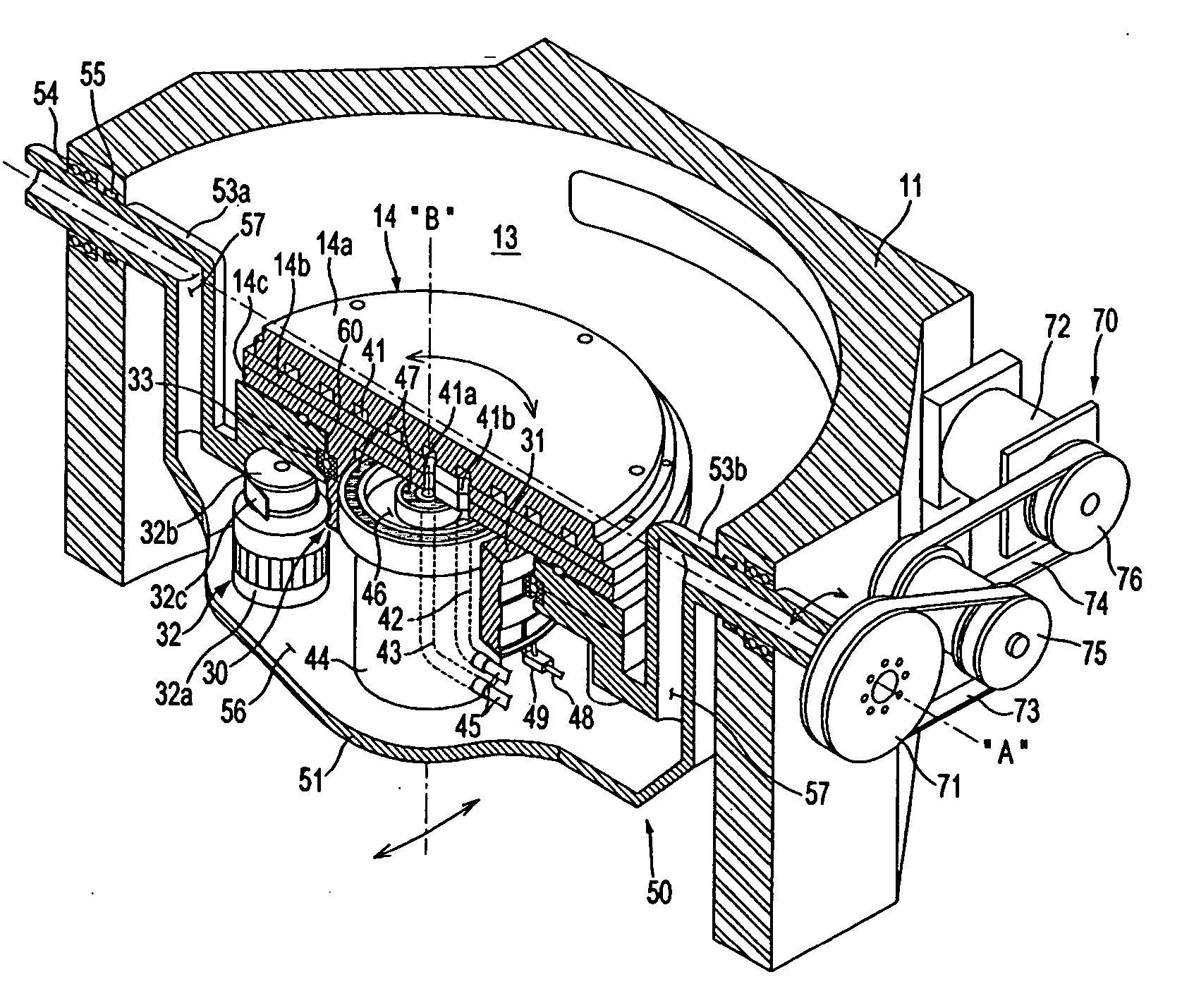
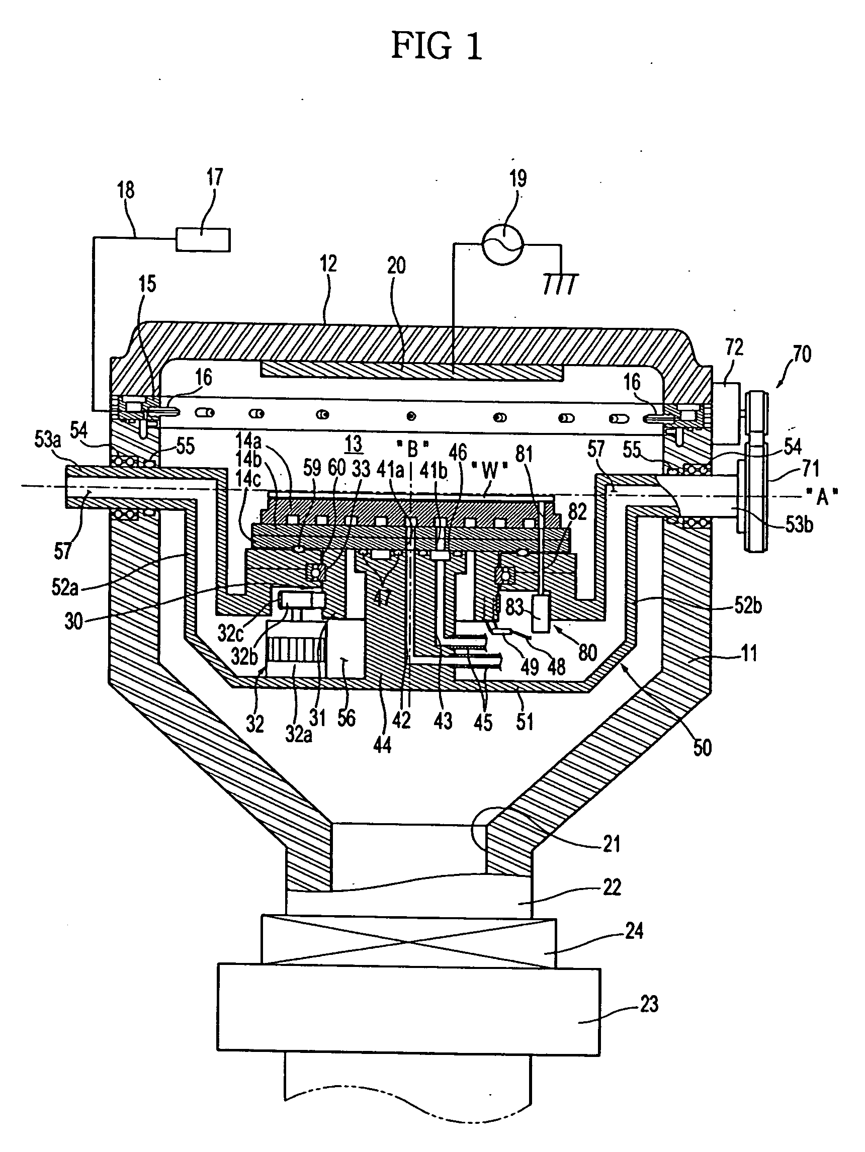
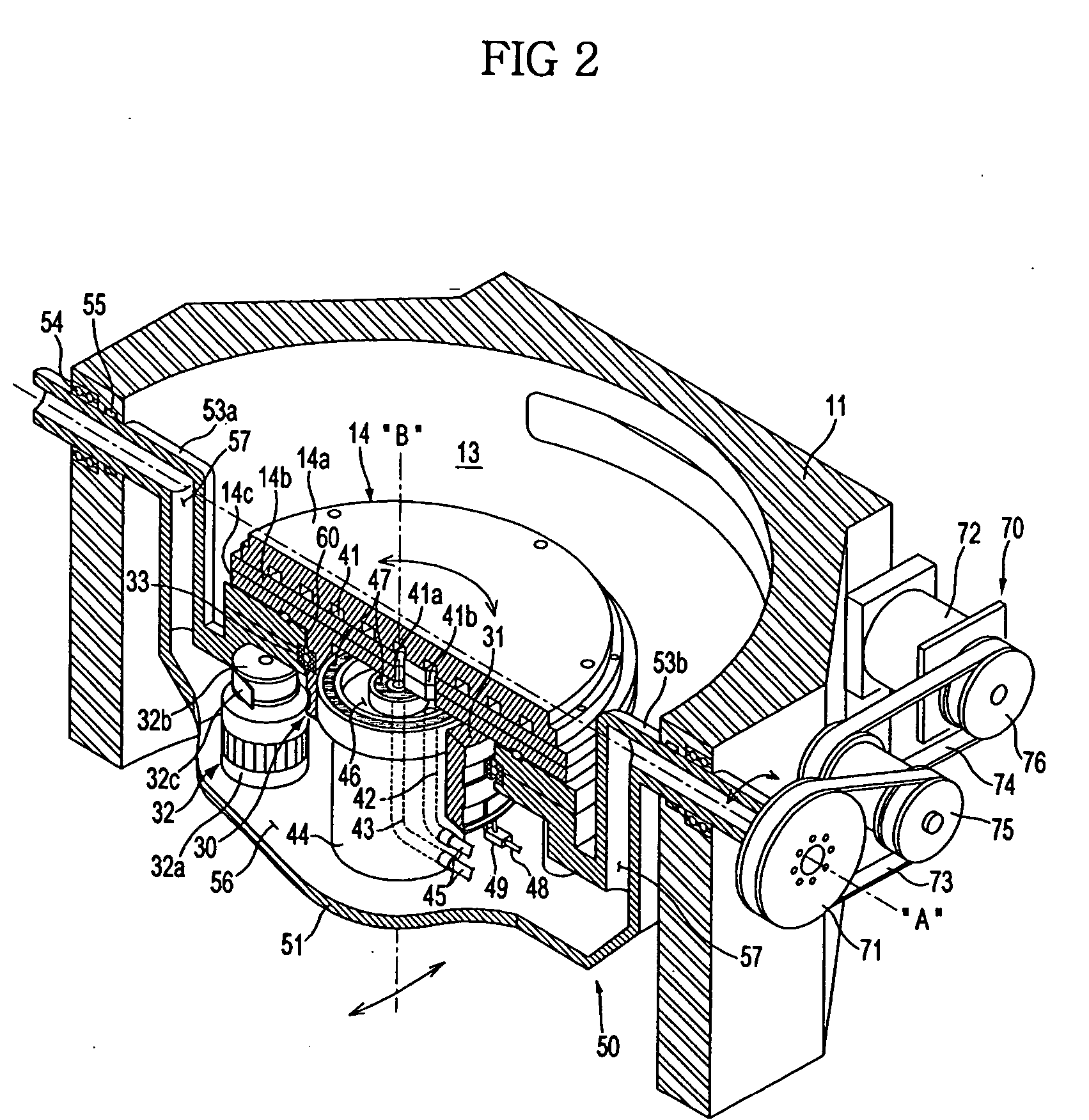
[0031]FIGS. 1-3 illustrate a semiconductor manufacturing apparatus according to an embodiment of the present general inventive concept. Referring to FIGS. 1-3, the semiconductor manufacturing apparatus includes a cylindrical body 11 open at an upper portion thereof and having a reaction chamber 13 to process a semiconductor wafer W therein, and a cover 12 to cover the open upper portion of the body 11.

[0032] A chuck 14 is provided within the reaction chamber 13 to support the semiconductor wafer W, and a gas distribution ring 15 is interposed between the upper surface of the body 11 and the cover 12. The gas distribution ring 15 includes a plurality of gas supply nozzles 16 to supply a processing gas ...


PUM


Abstract

A semiconductor manufacturing apparatus includes a body having a reaction chamber formed therein to process a semiconductor wafer, a chuck provided within the reaction chamber to support the semiconductor wafer, a chuck rotating device provided within the reaction chamber to support and rotate the chuck, and a slant adjuster to support the chuck rotating device and to adjust a position of the chuck rotating device to adjust a slant of an upper surface of the chuck.

Description

CROSS-REFERENCE TO RELATED APPLICATIONS [0001] This application claims the benefit under 35 U.S.C. §119 of Korean Patent Application No. 2005-6440, filed on Jan. 24, 2005, in the Korean Intellectual Property Office, the disclosure of which is incorporated herein in its entirety by reference. BACKGROUND OF THE INVENTION [0002] 1. Field of the Invention [0003] The present general inventive concept relates to a semiconductor manufacturing apparatus, and more particularly, to a semiconductor manufacturing apparatus designed to adjust a slant of a chuck to uniformly process a semiconductor wafer. [0004] 2. Description of the Related Art [0005] A conventional semiconductor manufacturing apparatus for performing a typical deposition or etching process is disclosed in U.S. Pat. No. 6,486,081. The conventional semiconductor manufacturing apparatus disclosed therein comprises a body including a reaction chamber in a vacuum state, a chuck provided within the reaction chamber to support a semic...

Claims


Application Information

Patent Timeline
Patent Type & Authority Applications(United States)
IPC IPC(8): B23Q1/00
CPCH01L21/68785H01L21/02H01L21/68
Inventor KIM, KYUNG SUNKIM, JUNG WOOKJEON, YUN KWANGLEE, JIN SEOK
Owner SAMSUNG ELECTRONICS CO LTD
Why Eureka
Try Eureka