Contact signal blocks for transmission of high-speed signals

a technology of contact signal blocks and high-speed signals, applied in the direction of coupling device connections, instruments, fault location, etc., can solve the problem of statistically more likely to occur, otherwise good chips to appear to be bad, and the real-world limit of approximately 200 defects per million opportunities (dmpo), so as to improve the conventional connectivity solution and keep the effect of separation

Inactive Publication Date: 2006-08-17
XANDEX
View PDF11 Cites 30 Cited by
  • Summary
  • Abstract
  • Description
  • Claims
  • Application Information

AI Technical Summary

Benefits of technology

[0005] According to the present invention, a variety of contact signal block architectures are provided which improve upon conventional connectivity solutions. According to a specific embodiment, a contact signal block for facilitating connections between test equipment and a device under test (DUT) is provided. The contact signal block includes a plurality of ground layers and a plurality of signal transmission layers disposed between and alternating with the ground layers. Each signal transmission layer includes a plurality of signal conductors. Each signal conductor forms a controlled-impedance transmission line with adjacent ground layers and is terminated at a first end in a plurality of signal spring probes. A plurality of non-conductive spacer structures separates the ground layers and signal transmission layers and maintains a substantially constant separation between the ground layers and the signal conductors. The ground layers and the signal conductors are primarily separated by a medium having a loss tangent of approximately 0.002 and a dielectric constant of less than about 1.5.

Problems solved by technology

Open or high impedance contacts can cause an otherwise good chip to appear to be bad, and are statistically more likely to occur as the number of signals increases.
Much time and effort has been expended improving the reliability of the spring probes (also known as Pogo™ pins) used to make these contacts, but there appears, at least for now, to be a real-world limit of approximately 200 defects per million opportunities (DMPO), a rate described in statistical terms as a failure rate of 5σ.
Since it is not possible to meet this standard with conventional spring probe solutions, techniques for achieving this standard are needed.

Method used


Image

  • Contact signal blocks for transmission of high-speed signals
  • Contact signal blocks for transmission of high-speed signals
  • Contact signal blocks for transmission of high-speed signals

Examples


Embodiment Construction

[0018] Reference will now be made in detail to specific embodiments of the invention including the best modes contemplated by the inventor for carrying out the invention. Examples of these specific embodiments are illustrated in the accompanying drawings. While the invention is described in conjunction with these specific embodiments, it will be understood that it is not intended to limit the invention to the described embodiments. On the contrary, it is intended to cover alternatives, modifications, and equivalents as may be included within the spirit and scope of the invention as defined by the appended claims. In the following description, specific details are set forth in order to provide a thorough understanding of the present invention. The present invention may be practiced without some or all of these specific details. In addition, well known features may not have been described in detail to avoid unnecessarily obscuring the invention.

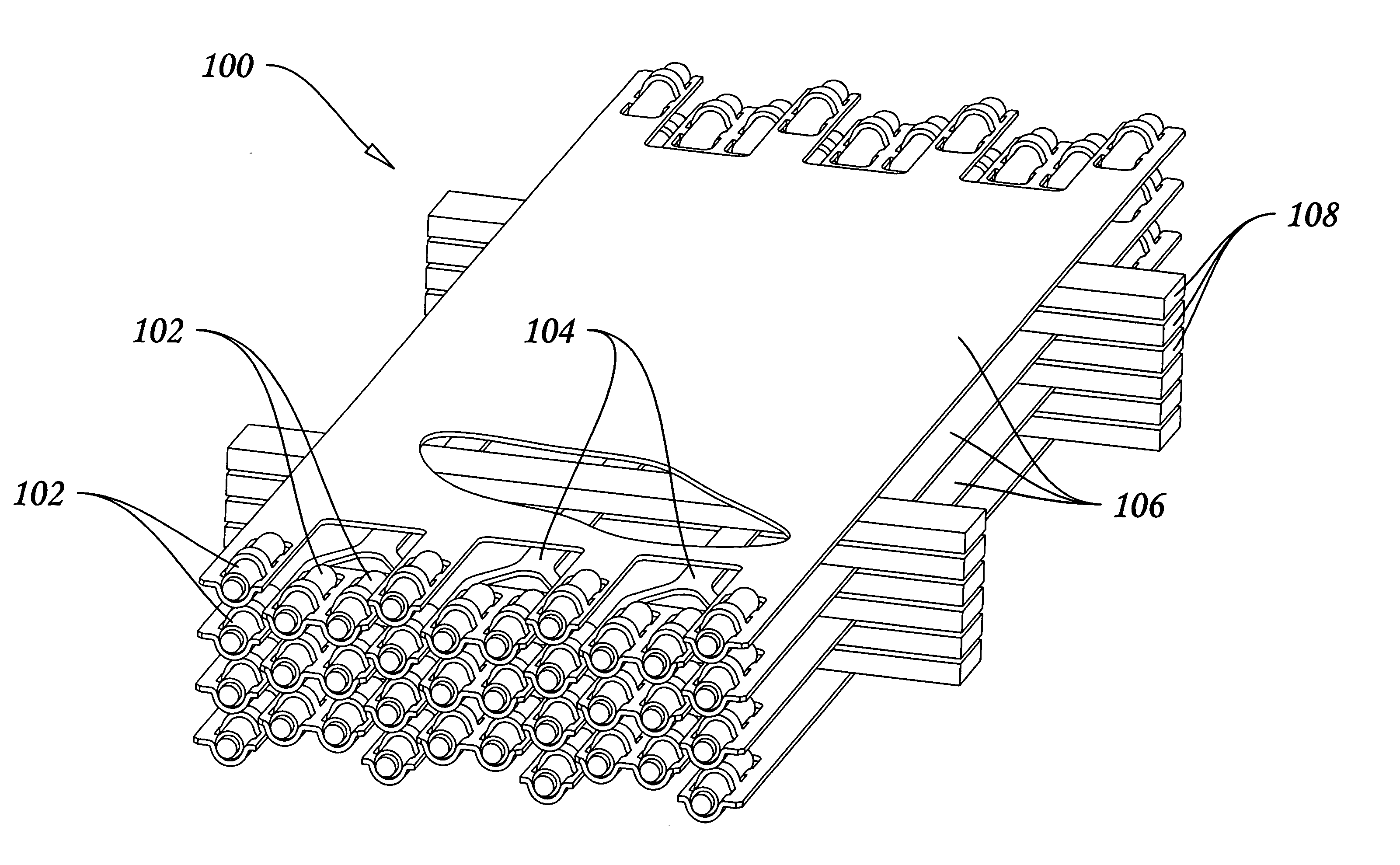
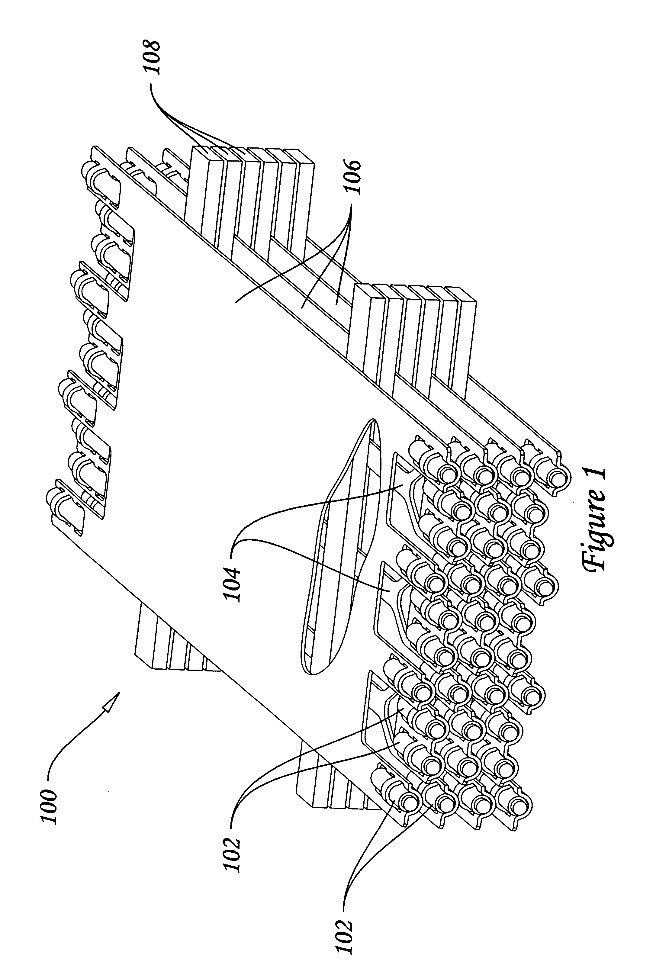
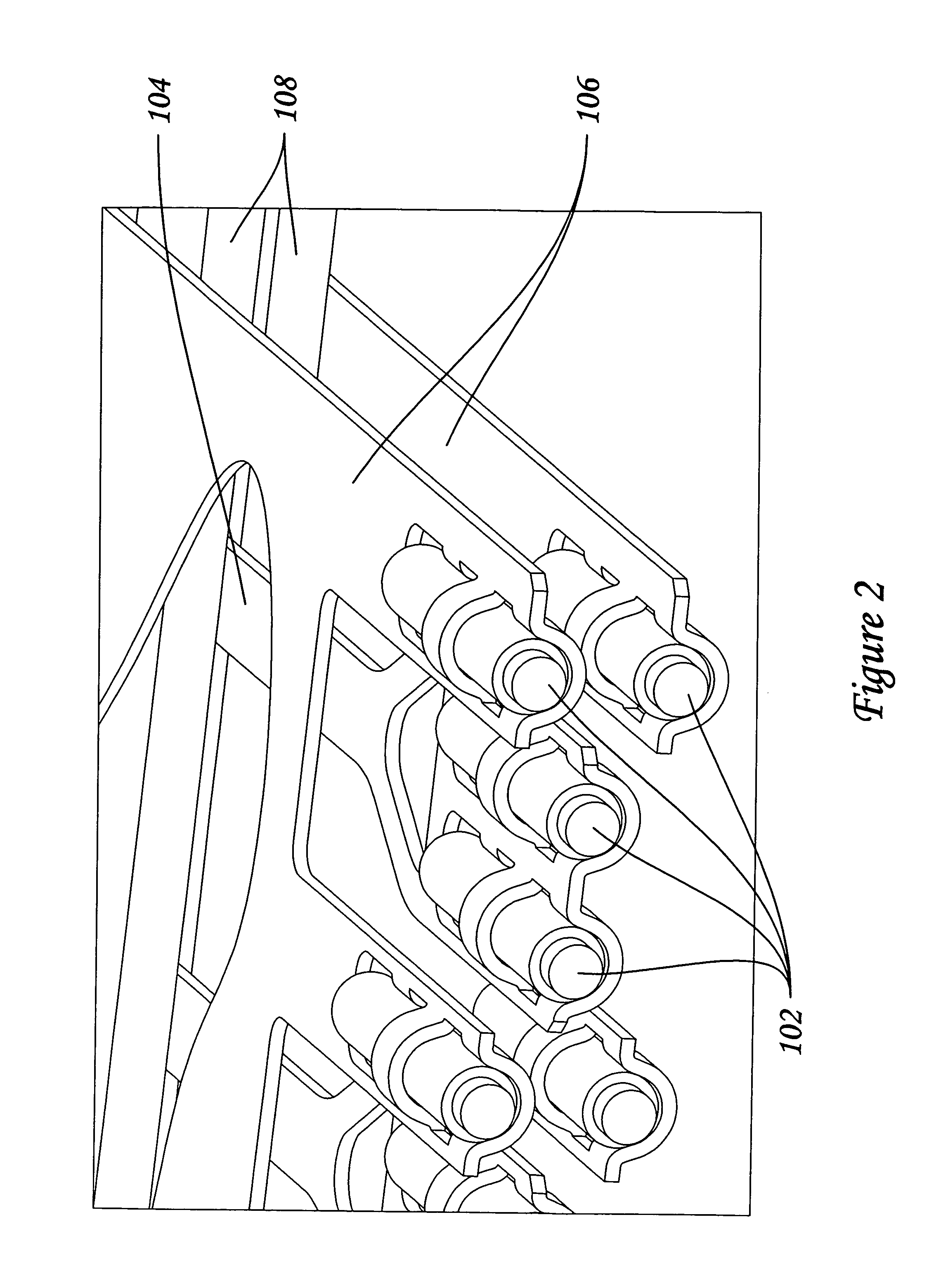
[0019] Embodiments of the present inven...


PUM


Abstract

A contact signal block for facilitating connections between test equipment and a device under test (DUT) is described. The contact signal block includes a plurality of ground layers and a plurality of signal transmission layers disposed between and alternating with the ground layers. Each signal transmission layer includes a plurality of signal conductors. Each signal conductor forms a controlled-impedance transmission line with adjacent ground layers and is terminated at a first end in a plurality of signal spring probes. A plurality of non-conductive spacer structures separates the ground layers and signal transmission layers and maintains a substantially constant separation between the ground layers and the signal conductors. The ground layers and the signal conductors are primarily separated by a medium having a loss tangent of approximately 0.002 and a dielectric constant of less than about 1.5.

Description

RELATED APPLICATION DATA [0001] The present application claims priority under 35 U.S.C. 119(e) to U.S. Provisional Patent Application No. 60 / 654,543 (Attorney Docket No. XANDP005P), and U.S. Provisional Patent Application No. 60 / 658,562 (Attorney Docket No. XANDP006P), the entire disclosures of both which are incorporated herein by reference for all purposes.BACKGROUND OF THE INVENTION [0002] The present invention relates to high-speed signal connections and, more specifically, to techniques for providing such connections between test equipment and devices under test (DUTs). [0003] As test systems use an increasing number of signals to test electronic devices and chips, the reliability of the connections between the test systems and the devices under test (DUTs) becomes increasingly critical. Open or high impedance contacts can cause an otherwise good chip to appear to be bad, and are statistically more likely to occur as the number of signals increases. Much time and effort has bee...

Claims


Application Information

Patent Timeline
Patent Type & Authority Applications(United States)
IPC IPC(8): H01R13/648
CPCG01R1/0408G01R1/06772H01R13/2471H01R13/514H01R13/65807H01R2201/20H01R13/6471H01R13/6477H01R13/6589
Inventor SINSHEIMER, ROGER
Owner XANDEX
Why Eureka
Try Eureka