Electro-optic device and electronic instrument

a technology of electro-optic devices and electronic instruments, applied in the direction of static indicating devices, non-linear optics, instruments, etc., can solve the problems of problematic inhibiting high-definition display, fluctuation of the boundary between the area with the first grayscale and the area with the second grayscale by the electric field in the tilted direction,

Active Publication Date: 2006-08-24
E INK CORPORATION
View PDF9 Cites 18 Cited by
  • Summary
  • Abstract
  • Description
  • Claims
  • Application Information

AI Technical Summary

Problems solved by technology

As a result, the black electrophoretic particles moving closer to the second substrate 20 are distributed in an area Rb larger than an area R. Therefore, a high-definition display is problematically inhibited.
Note that, although the electro-optic device utilizing the electrophoretic particles is particularly described here, the same problem can arise in electro-optic devices utilizing other electro-optic materials such as liquid crystal.
No

Method used


Image

  • Electro-optic device and electronic instrument
  • Electro-optic device and electronic instrument
  • Electro-optic device and electronic instrument

Examples


first embodiment

A: First Embodiment

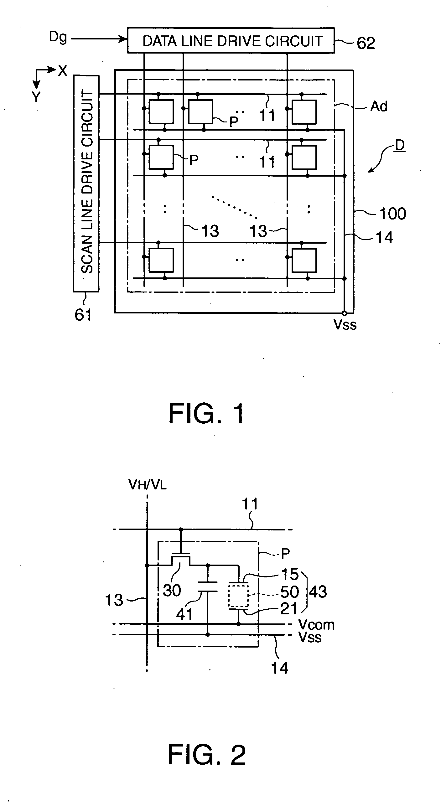
[0037]FIG. 1 is a block diagram showing an electrical configuration of an electro-optic device according to a first embodiment of the invention. As shown in the figure, the electro-optic device D includes an electro-optic panel 100 for displaying images in a display area Ad, and a scan line drive circuit 61 and a data line drive circuit 62 both for driving the electro-optic panel 100. The electro-optic panel 100 includes a plurality of scan lines 11 extending in the X direction and connected to the scan line drive circuit 61, a plurality of data lines 13 extending in the Y direction perpendicular to the X direction and connected to the data line drive circuit 62, and a power supply line 14 supplied with a predetermined electric potential Vss. A pixel P is disposed at an intersection of each of the scan lines 11 and each of the data lines 13. Therefore, these pixels P are arranged in a matrix in both the X direction and the Y direction throughout the display area A...

second embodiment

B: Second Embodiment

[0055] A second embodiment of the invention will hereinafter be described.

[0056] In the first embodiment, the configuration for displaying two levels of grayscales, black and white, using each of the pixels P as a unit of display is described as an example. On the contrary, a configuration capable of displaying halftone in addition to black and white using an area modulation method defining a set of plural pixels P as a unit of display is adopted in the present embodiment. Note that in the present embodiment, elements having the same functions and operations as those in the first embodiment are provided with common reference numerals and the descriptions therefor may be omitted if appropriate.

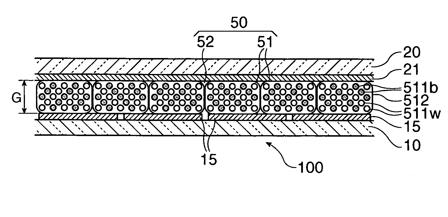
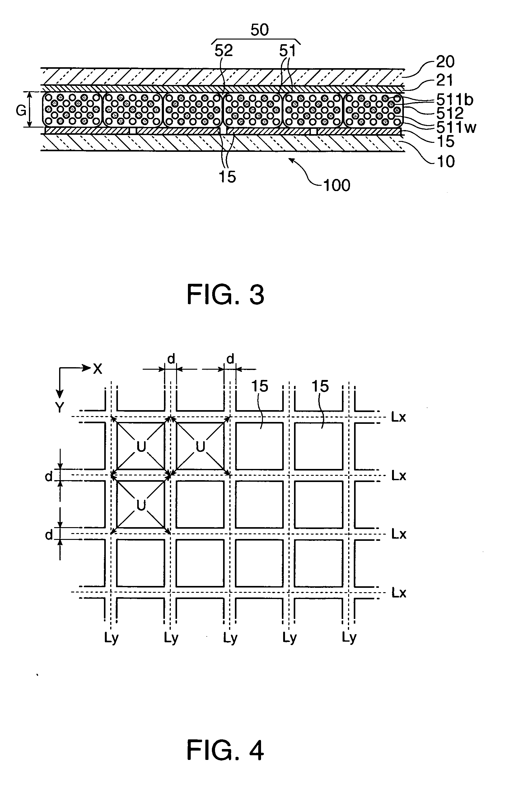
[0057]FIG. 13 is a plan view showing the arrangement of the pixel electrodes 15 in the present embodiment. As shown in the figure, in the present embodiment, five levels of grayscale is displayed by the area modulation method using a set (hereinafter referred to as a unit ...

modified embodiment 1

[0064] Although the configuration in which the electrophoretic dispersion liquid (the dispersion medium 512 dispersing the electrophoretic particles 511) is encapsulated in the microcapsule 51 is exemplified in each of the embodiments, a configuration in which the electrophoretic dispersion liquid is directly sealed in a gap between the first substrate 10 and the second substrate 20 can also be adopted, or a configuration in which the gap between the first substrate 10 and the second substrate 20 is partitioned by partitions (not shown) into a number of microscopic chambers each encapsulating the electrophoretic dispersion liquid can also be adopted. Further, although the configuration in which two kinds of electrophoretic particles 511 each having different color from the other is dispersed in the dispersion medium 512 is exemplified in each of the embodiments, a configuration in which the dispersion medium 512 provided with a specific color disperses a single kind of electrophoret...


PUM


Abstract

An electro-optic device includes a plurality of pixel electrodes each formed for respective unit areas with a distance between one of the pixel electrodes and another of the pixel electrodes adjacent to the one of the pixel electrodes, the unit areas being arranged in a plane and defined by dividing the plane into the same shapes without a gap, and an electro-optic layer that faces each of the pixel electrodes, and in response to application of a first electric potential to each of the pixel electrodes, expresses a first grayscale in an area corresponding to each of the pixel electrodes, in response to application of a second electric potential different form the first electrical potential to each of the pixel electrodes, expresses a second grayscale different from the first grayscale in an area corresponding to each of the pixel electrodes, wherein the distance between one of the pixel electrodes and another of the pixel electrodes adjacent to the one of the pixel electrodes is selected so that a boundary between an area expressing the first grayscale in response to application of the first electric potential to the one of the pixel electrodes and an area expressing the second grayscale in response to application of the second electric potential to the another of the pixel electrodes adjacent to the one of the pixel electrodes is substantially identical to a boundary between the unit area provided with the one of the pixel electrodes and the unit area provided with the another of the pixel electrodes.

Description

BACKGROUND OF THE INVENTION [0001] 1. Technical Field [0002] The present invention relates to a technology for controlling the behavior of various kinds of electro-optic materials such as charged microparticles (hereinafter referred to as electrophoretic particles) by applying them with voltages. [0003] 2. Related Art [0004] The electro-optic devices utilizing these kinds of electro-optic materials have been conventionally proposed as display devices for various electronic instruments. For example, JPA-2004-4714 (Paragraph No. 0103 and FIG. 1) and JPA-2003-84314 (Paragraph No. 0003 and FIG. 9) disclose an electro-optic device having an electro-optic layer 50 intervening in a gap between a first substrate 10 and a second substrate 20 facing each other as shown in FIG. 19. The electro-optic layer 50 is a layer in which positively charged black electrophoretic particles and negatively charged white electrophoretic particles are dispersed in a dispersion medium (both omitted from the dr...

Claims


Application Information

Patent Timeline
IPC IPC(8): G09G3/34G02F1/167G02F1/1676G02F1/16766
CPCG02F1/167G02F2001/1676G09G3/344G09G2310/061G02F1/1676G02F1/16766
Inventor KOMATSU, YUKO
Owner E INK CORPORATION
Why Eureka
Try Eureka