
Red phosphorescene compounds and organic electroluminescence device using the same
- Summary
- Abstract
- Description
- Claims
- Application Information
AI Technical Summary
Benefits of technology
Problems solved by technology
Method used
Image

Examples
embodiments
1. First Embodiment
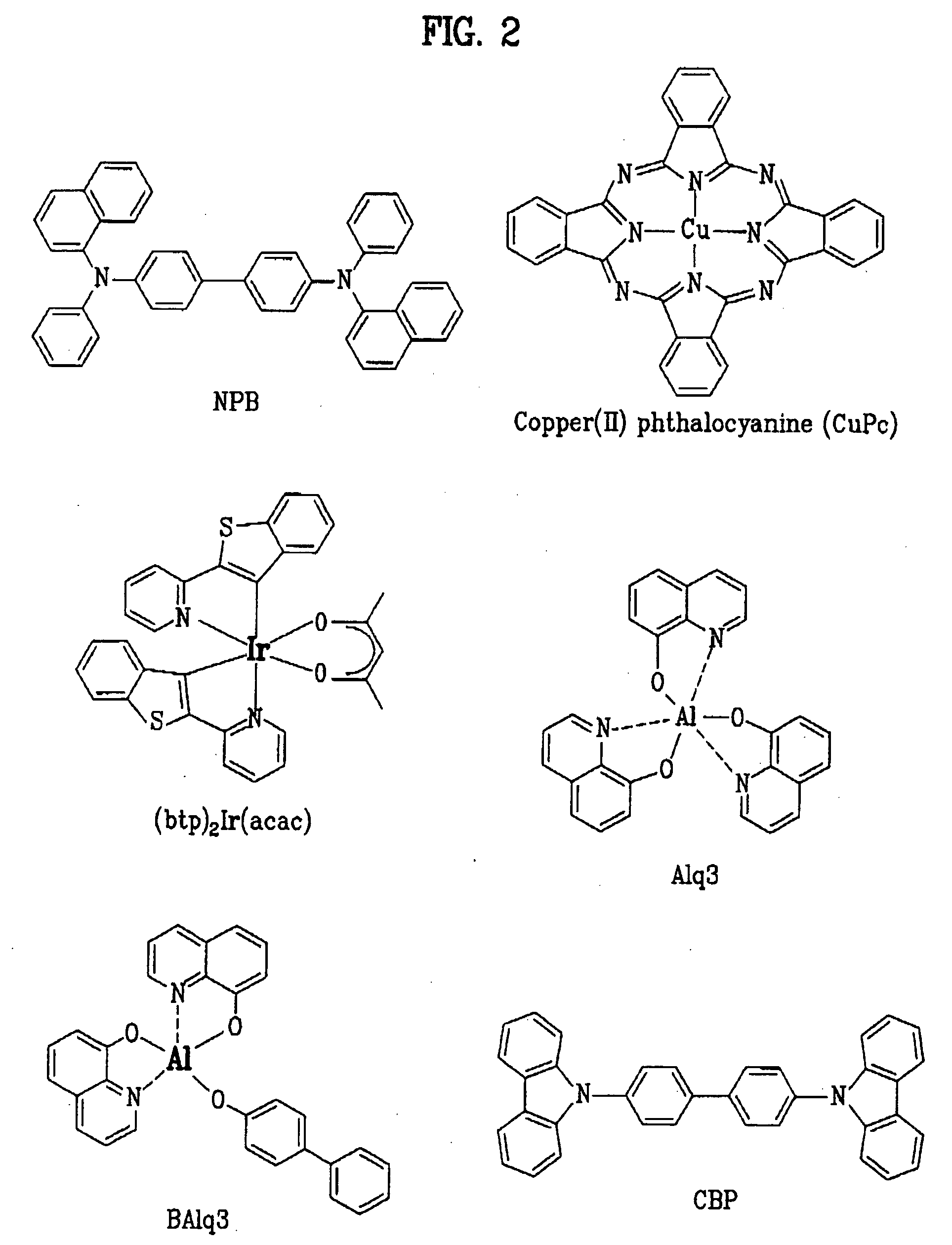
[0037] An ITO glass substrate is patterned to have a light emitting area of 3 mm×3 mm. Then, the patterned ITO glass substrate is washed. Subsequently, the substrate is mounted on a vacuum chamber. The standard pressure is set to 1×10⁻⁶ torr. Thereafter, layers of organic matter are formed on the ITO substrate in the order of CuPC (200 Å), NPB (400 Å), CBP+(btp)2Ir(acac)(7%) (200 Å), a hole blocking layer (100 Å), Alq3 (300 Å), LiF (5 Å), and Al (1000 Å).
[0038] When forming a hole blocking layer using BAlq, the brightness is equal to 689 cd / m2 (8.1 V) at 0.9 mA. At this point, CIE x=0.651, y=0.329. Furthermore, the durability (half of the initial brightness) lasts for 1600 hours at 2000 cd / m2.
second embodiment
2. Second Embodiment
[0039] An ITO glass substrate is patterned to have a light emitting area of 3 mm×3 mm. Then, the patterned ITO glass substrate is washed. Subsequently, the substrate is mounted on a vacuum chamber. The standard pressure is set to 1×10⁻⁶ torr. Thereafter, layers of organic matter are formed on the ITO substrate in the order of CuPC (200 Å), NPB (400 Å), BAlq+A-2(7%) (200 Å), Alq3 (300 Å), LiF (5 Å), and Al (1000 Å).
[0040] At 0.9 mA, the brightness is equal to 1448 cd / m2 (6.2 V). At this point, CIE x=0.644, y=0.353. Furthermore, the durability (half of the initial brightness) lasts for 8000 hours at 2000 cd / m2.
third embodiment
3. Third Embodiment
[0041] An ITO glass substrate is patterned to have a light emitting area of 3 mm×3 mm. Then, the patterned ITO glass substrate is washed. Subsequently, the substrate is mounted on a vacuum chamber. The standard pressure is set to 1×10⁻⁶ torr. Thereafter, layers of organic matter are formed on the ITO substrate in the order of CuPC (200 Å), NPB (400 Å), BAlq+A-5(7%) (200 Å), Alq3 (300 Å), LiF (5 Å), and Al (1000 Å).
[0042] At 0.9 mA, the brightness is equal to 1378 cd / m2 (6.0 V). At this point, CIE x=0.659, y=0.351. Furthermore, the durability (half of the initial brightness) lasts for 7000 hours at 2000 cd / m2.
PUM
| Property | Measurement | Unit |
|---|---|---|
| Length | aaaaa | aaaaa |
| Length | aaaaa | aaaaa |
| Length | aaaaa | aaaaa |
Abstract
Description
Claims
Application Information