

Optical scanning device, image forming apparatus, and method of reducing noises in optical scanning device
a scanning device and optical technology, applied in the field of optical scanning devices, can solve the problems of large image forming apparatus, and high cost of individual optical scanning devices for each image holding member, so as to reduce noise, reduce noise, and reduce noise
- Summary
- Abstract
- Description
- Claims
- Application Information
AI Technical Summary
Benefits of technology
Problems solved by technology
Method used
Image

Examples
first embodiment
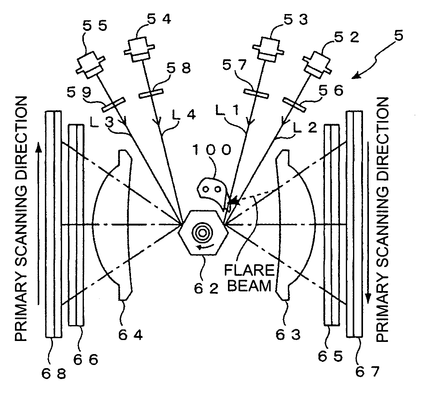
[0061] A first embodiment according to the present invention will be explained with reference to FIGS. 1 through 13.
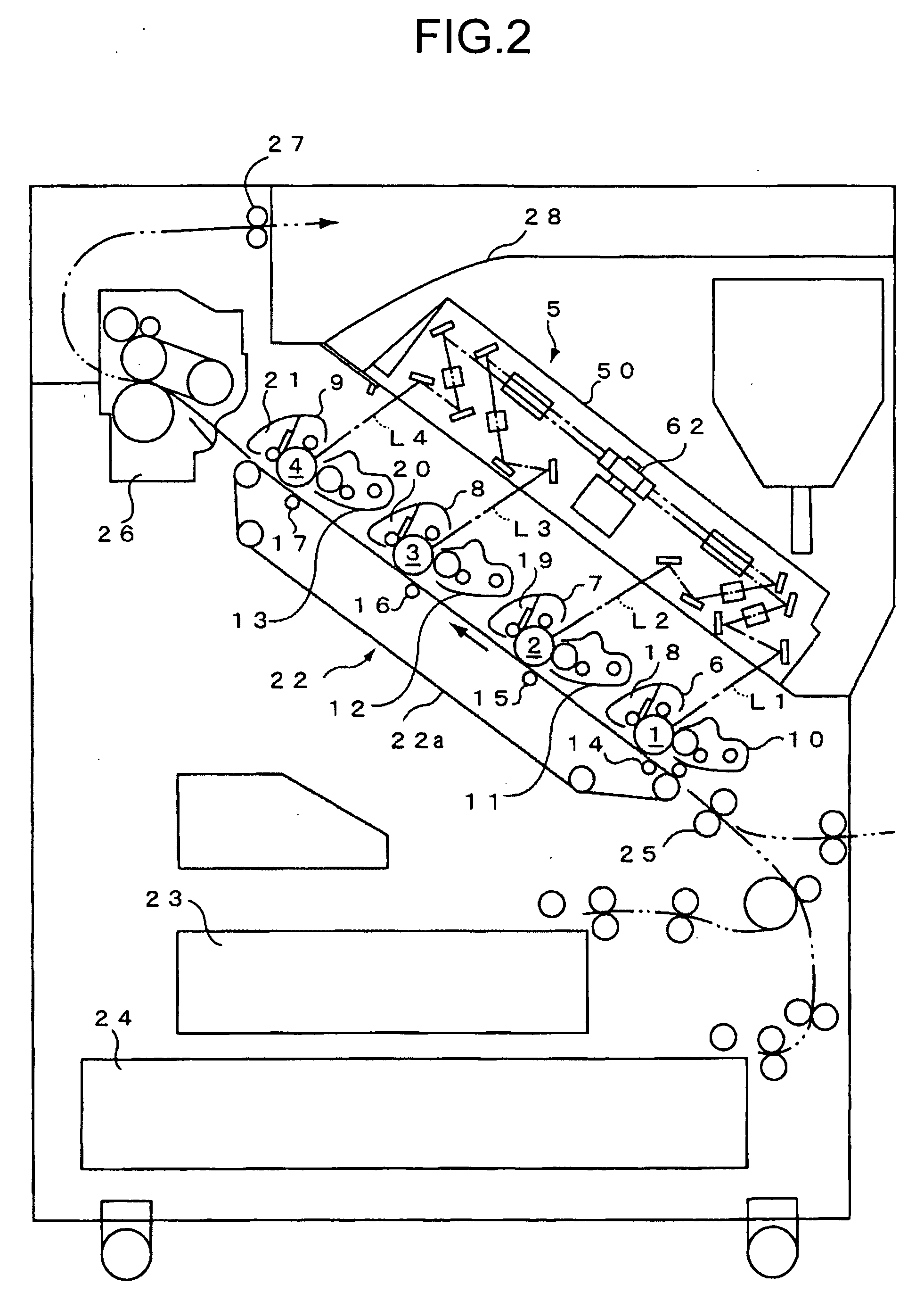
[0062] The general structure and operations of an image forming apparatus according to the present embodiment will be explained with reference to FIG. 2. The image forming apparatus is a full-color image forming apparatus in which a plurality of optically-conductive photosensitive members in the form of drums (namely, photosensitive drums) 1, 2, 3, and 4 are disposed next to one another so as to serve as image holding members. These four photosensitive drums 1, 2, 3, and 4 form images corresponding to the colors of yellow (Y), magenta (M), cyan (C), and black (Bk), respectively, starting from the one on the right side of the page, for example. It should be noted that the order in which the colors are arranged is not limited to this example and can be arranged in any other way.
[0063] In order to perform an electronic photograph process, around the four photosensitive d...
third embodiment
[0129]FIGS. 15 and 16 are drawings for illustrating the present invention.
[0130] In the third embodiment, the characteristics lie in that the edge line portions 101b and 102b of the flare beam shielding member 100 that come closest to an edge portion 113g of a polygon mirror 113, which is made of one stage having a larger thickness in the secondary scanning direction, are arranged to be positioned at a torsional angle (including the concept of inclination) with respect to the edge portion 113g of the polygon mirror 113.
[0131] By having this arrangement, because the inside surfaces of the edge line portions 101b and 102b are inclined, the area compressed between the edge line portions 101b and 102b and the edge portion 113g of the polygon mirror 113 is reduced.
[0132] In addition, as shown in FIG. 16 (a view of the flare beam shielding member 100 seen from the direction of the polygon mirror 113), because the edge lines 101a and 102a are inclined substantially in the rotation direct...
fourth embodiment
[0134]FIG. 17 is a drawing for illustrating the present invention.
[0135] According to the fourth embodiment, the characteristics lie in that the polygon edge portion and the edge line portion of the flare beam shielding member 100 in the secondary scanning direction are arranged so that they do not pass each other with a substantially constant distance therebetween for the whole area in the secondary scanning direction.
[0136] As shown in FIG. 17, the flare beam shielding member 100 is not divided into an upper portion and a lower portion, but rather has only an edge line portion 100b that includes an edge line 100a. The edge line 100a is inclined so that it is not parallel to the edge line of the edge portion 113g of the polygon mirror 113. Because the distance between the polygon edge portion and the edge line portion 100b changes in the secondary scanning direction (i.e. the distance gets larger toward the upper direction), it is possible to avoid the situation where rapid compre...
PUM
 Abstract
Description
Claims
Application Information