Liquid crystal display device
- Summary
- Abstract
- Description
- Claims
- Application Information
AI Technical Summary
Benefits of technology
Problems solved by technology
Method used
Image

Examples
first embodiment
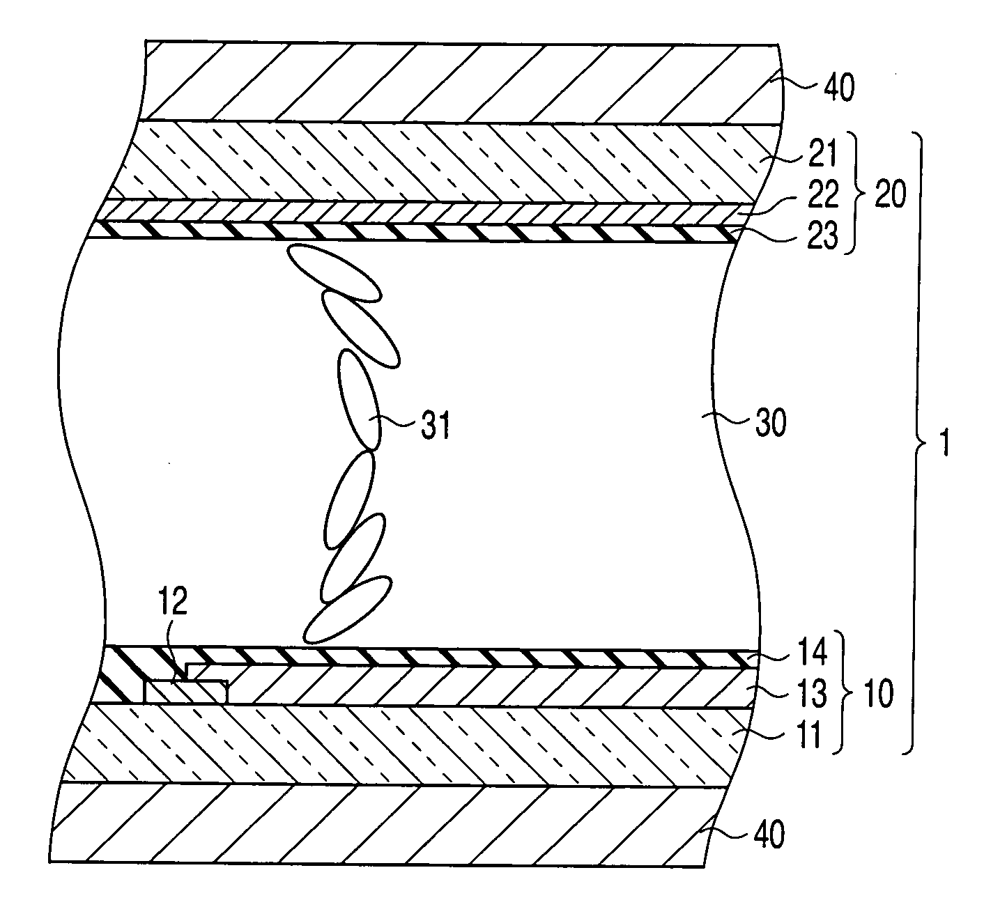
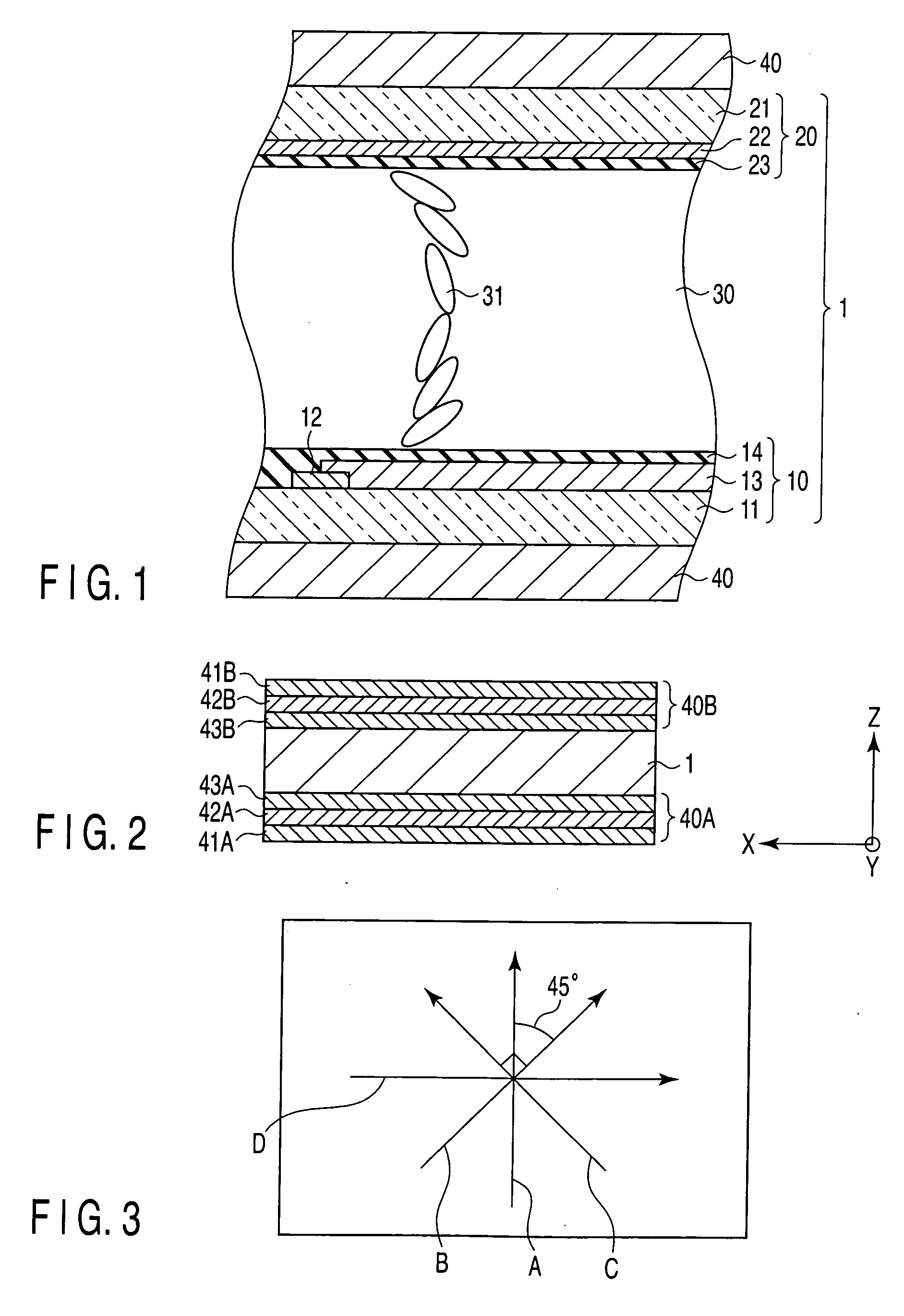
[0059] As is shown in FIG. 7, in an OCB liquid crystal display device according to a first embodiment, optical compensation elements 40A and 40B are provided on the array substrate (10)-side outer surface of the liquid crystal panel 1 and on the opposed substrate (20)-side outer surface of the liquid crystal panel 1.
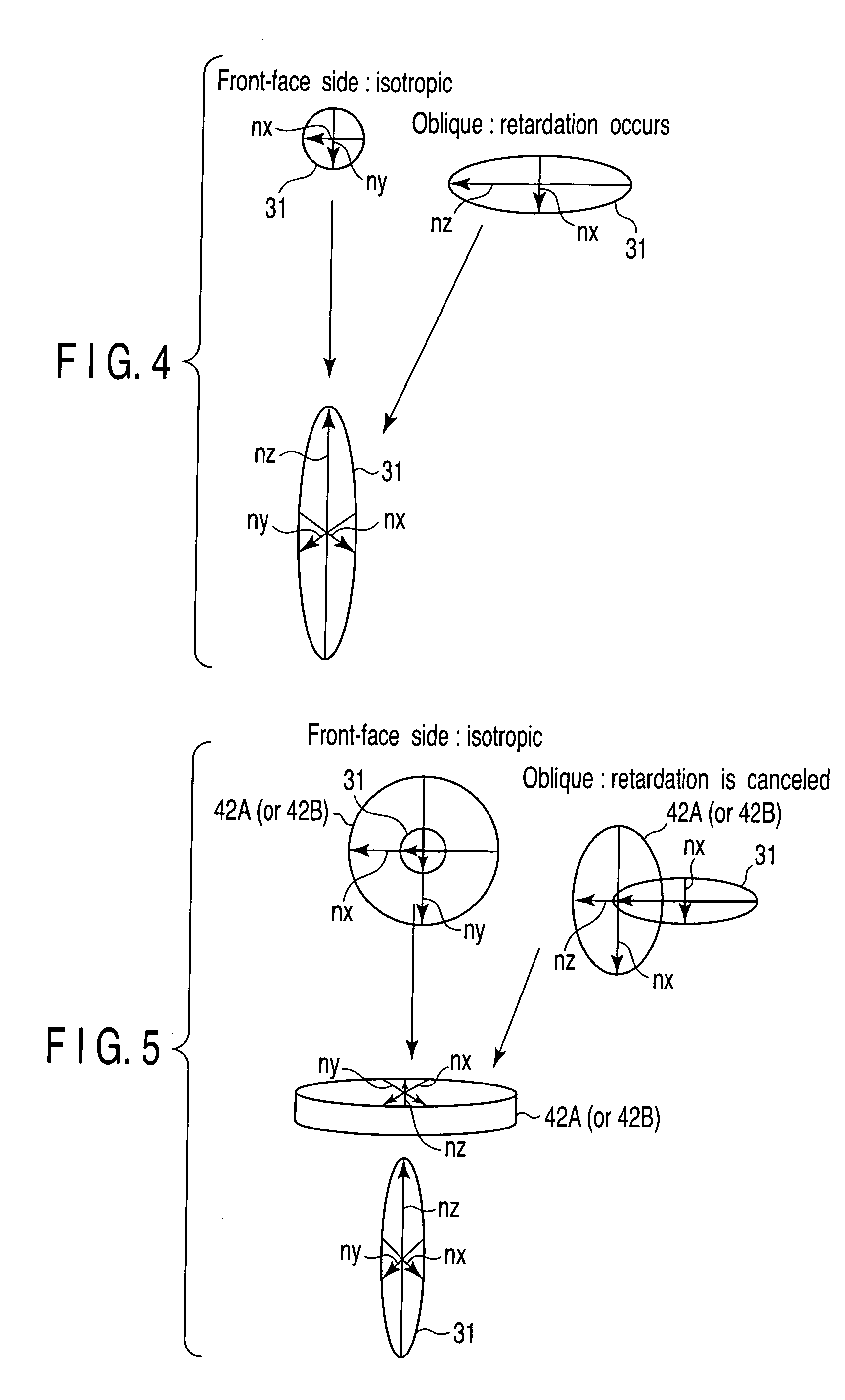
[0060] The optical compensation element 40A on the array substrate 10 side includes a polarizer plate 41A, a phase plate 42A having retardation in its thickness direction, a first phase plate 43A having retardation in its front-plane direction, and a second phase plate 44A having retardation in its front-plane direction. Similarly, the optical compensation element 40B on the opposed substrate 20 side includes a polarizer plate 41B, a phase plate 42B having retardation in its thickness direction, a first phase plate 43B having retardation in its front-plane direction, and a second phase plate 44B having retardation in its front-plane direction. The transmission-axis dire...
second embodiment
[0073] As is shown in FIG. 9, like the first embodiment, in an OCB liquid crystal display device according to a second embodiment, optical compensation elements 40A and 40B are provided on the array substrate (10)-side outer surface of the liquid crystal panel 1 and on the opposed substrate (20)-side outer surface of the liquid crystal panel 1. The structural components common to those in the first embodiment are denoted by like reference numerals, and a detailed description thereof is omitted.
[0074] The optical compensation element 40A on the array substrate 10 side includes a polarizer plate 41A, a phase plate 42A having retardation in its thickness direction, a first phase plate 43A having retardation in its front-plane direction, and a second phase plate 44A having retardation in its front-plane direction. On the other hand, the optical compensation element 40B on the opposed substrate 20 side includes a polarizer plate 41B, a phase plate 42B having retardation in its thickness...
third embodiment
[0079] As is shown in FIG. 10, like the first embodiment, in an OCB liquid crystal display device according to a third embodiment, optical compensation elements 40A and 40B are provided on the array substrate (10)-side outer surface of the liquid crystal panel 1 and on the opposed substrate (20)-side outer surface of the liquid crystal panel 1. The structural components common to those in the first embodiment are denoted by like reference numerals, and a detailed description thereof is omitted.
[0080] The optical compensation element 40A on the array substrate 10 side includes a polarizer plate 41A, a phase plate 42A having retardation in its thickness direction, and a first phase plate 43A having retardation in its front-plane direction. On the other hand, the optical compensation element 40B on the opposed substrate 20 side includes a polarizer plate 41B, a phase plate 42B having retardation in its thickness direction, and a second phase plate 44B having retardation in its front-p...
PUM
 Abstract
Description
Claims
Application Information
PatSnap Eureka turns technology decisions into work you can execute. Powered by our Innovation Knowledge Graph, it runs expert workflows across engineering, life sciences, materials and intellectual property. Get your review-ready output in minutes.


