

Display device
- Summary
- Abstract
- Description
- Claims
- Application Information
AI Technical Summary
Benefits of technology
Problems solved by technology
Method used
Image

Examples
first embodiment
[0038] Embodiments of the present invention will now be described with reference to the accompany drawings. The following description shows the preferred embodiments of the present invention, however the scope of the present invention is not limited by the following embodiments. In the following description, composing elements denoted with a same reference symbol substantially have the same content.
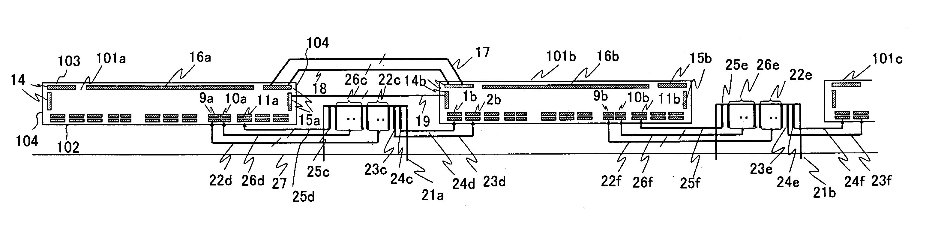
[0039] The configuration of the liquid crystal display panel 33 of the liquid crystal display device will now be described with reference to FIG. 1. FIG. 1 is a top view depicting the configuration of the liquid crystal display panel in the COG packaging type liquid crystal display device. The liquid crystal display panel 33 shown in FIG. 1 is comprised of a display area 34 which is further comprised of a plurality of pixels arrayed in a matrix, and a screen border area 35 outside of the display area 34. The liquid crystal display panel 33 is comprised of an array substrate where an arra...
second embodiment
[0067] The present embodiment will be described with reference to FIG. 10. FIG. 10 is a plan view depicting the configuration of the area around the bumps for input provided on the source driver IC of the liquid crystal display device. Compared with the first embodiment, the configuration between the FPC 21 and the bumps for input is different in the present embodiment, and description will be omitted for the configuration the same as the first embodiment.
[0068] In the present embodiment, in the FPC 21, the terminal for GND 24c and the terminal for analog power supply 23c are connected to the source driver IC 101b at the right, and the terminal for digital power supply 25c, the terminal for reference voltage at the positive polarity side 22c and the terminal for reference voltage at the negative polarity side 26c are connected with the source driver IC 101a at the left. By providing the terminal for digital power supply 25c at the left of the FPC 21, the line width of the GND 24d a...
third embodiment
[0071] The present embodiment will be described with reference to FIG. 11. FIG. 11 is a plan view depicting the configuration of the area around the bumps for input provided on the source driver IC of the liquid crystal display device. Compared with the first embodiment, the configuration between the FPC 21 and the bumps for input is different in the present embodiment, and description will be omitted for the configuration the same as the first embodiment.
[0072] According to the present embodiment, an FPC 21 is mounted at every other space between the source driver ICs, so that one FPC 21 is connected to two source driver ICs. This FPC 21a supplies all the signals and power for operating both the source driver IC 101a and the source driver IC 101b at the left and right. In other words, terminals for connecting with the source driver IC 101a are provided in the side section at the left of the FPC 21, which connect with the respective bumps for input of the source driver IC 101a via ...
PUM
 Abstract
Description
Claims
Application Information