Eureka AIR delivers breakthrough ideas for toughest innovation challenges, trusted by R&D personnel around the world.

Substrate for liquid crystal display device and liquid crystal display device including the same

Active Publication Date: 2009-04-30
SHARP KK
View PDF5 Cites 3 Cited by
  • Summary
  • Abstract
  • Description
  • Claims
  • Application Information

AI Technical Summary

Benefits of technology

[0024]According to the invention, it is possible to embody a liquid crystal display device having an excellent display quality and a substrate used for the liquid crystal display device.

Problems solved by technology

However, spacers dispersed within a pixel can cause an alignment defect of the liquid crystal and leakage of light.
An alignment defect or leakage of light results in a reduction of contrast or glare on the display screen, which degrades display quality.
Further, increases in the size of substrates have made it difficult to disperse spacers evenly.
When spacers are unevenly dispersed, the cell thickness between the substrates can vary to result in irregularities of luminance.
At a liquid crystal filling and sealing step utilizing a dip type vacuum filling process, a panel which has been filled with a liquid crystal is pressed from the outside at a predetermined pressure to eject any extra part of the liquid crystal, whereby the cell thickness is adjusted However, when the pillar spacer 146 is too hard, the pillar spacer 146 cannot be sufficiently shrunk even if they are pressed at the predetermined pressure.
As a result, the liquid crystal is moved toward a lower part of the panel by gravity, and an irregularity is therefore caused by gravity in that the cell thickness becomes greater in the lower part.
When the pillar spacer 146 is too soft, since they undergo a great amount of displacement and also a great amount of plastic deformation in response to a pressure from the outside, an irregularity of the cell thickness can occur.

Method used


Image

  • Substrate for liquid crystal display device and liquid crystal display device including the same
  • Substrate for liquid crystal display device and liquid crystal display device including the same
  • Substrate for liquid crystal display device and liquid crystal display device including the same

Examples


example 1

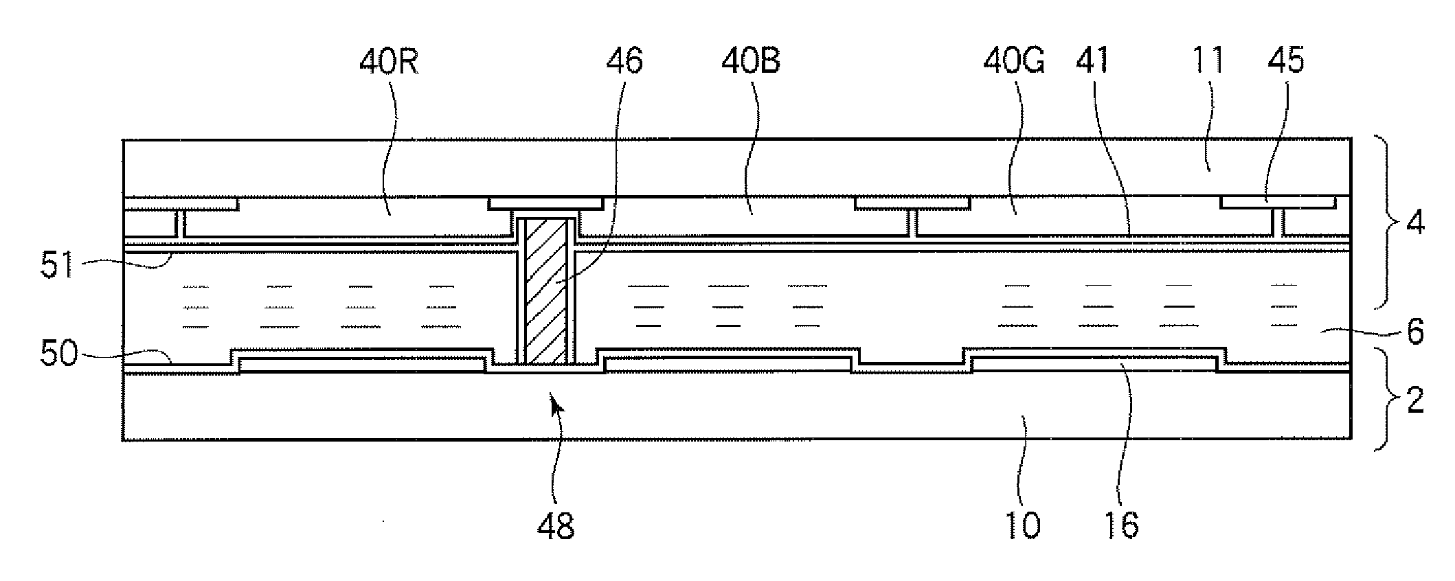
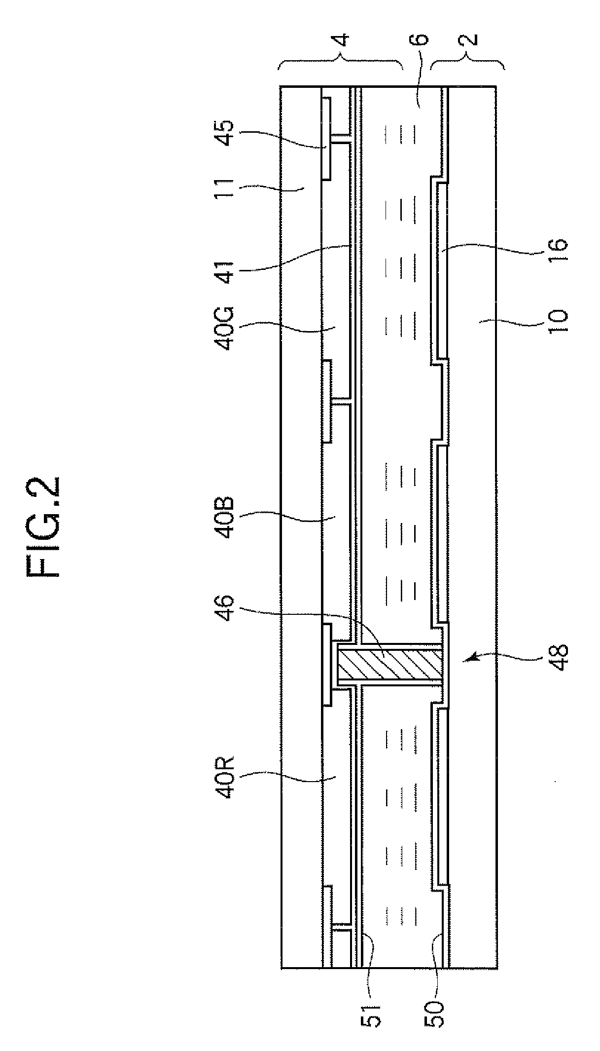
[0033]An example of forming the resin spacer layer 46 on the CF substrate 4 side will be described. FIG. 5 is a diagram illustrating a configuration of a manufactured CF substrate 4, and FIGS. 6(a) to (d) are process sectional views of a portion cut along the line A-A in FIG. 5. First, a low-reflective Cr film (a film thickness of 0.2 μm) is coated on the transparent glass substrate 11 illustrated in FIG. 6(a). Next, a resist mask is formed by coating a photo resist thereon, exposing and developing the photo resist. The Cr film is etched by using the resist mask, and then the resist mask is removed, whereby the BM 45 is formed as shown in FIG. 6(a).

[0034]Next, as shown in FIG. 6(b), an R resist (a film thickness of 1.8 μm) of a photosensitive pigment dispersion type is coated and patterned, and then a CF resin layer 40R is formed on an R pixel portion. Next, a G resist (a film thickness of 1.8 μm) of a photosensitive pigment dispersion type is coated and patterned, and then a CF res...

example 2

[0040]An alignment film 51 was formed on the surface of the CF substrate 4 according to the example 1, and an alignment film 50 was formed on the surface of the TFT substrate 2 manufactured through predetermined processes. After that, a liquid crystal display device of a TN mode as shown in FIG. 2 was manufactured through processes such as a rubbing process, a seal forming process, an assembly process, a cutting process, a liquid crystal filling process, a sealing process, and a polarizer attachment process.

[0041]Since an organic film other than the alignment film 50 is not formed on the TFT substrate 2 side of the manufactured liquid crystal display device, the structure 48 has a structure not including organic materials other than the resin spacer layer 46 and the alignment films 50 and 51. The alignment films 50 and 51 have a very small film thickness of about 0.1 μm, and the films have almost no influence on the characteristics of the structure 48. For this reason, the structure...

example 3

[0042]An example of applying the embodiment to a liquid crystal display device of MVA mode will be described. FIG. 8 shows a sectional configuration of a liquid crystal display device according to the example. As shown in FIG. 8, a linear protrusion 54 is formed as an alignment regulating structure for regulating an alignment direction of the liquid crystal 6 on the CF substrate 4. A slit (in which the ITO film is removed) 52 is formed as an alignment regulating structure on the TFT substrate 2. For example, the liquid crystal 6 has a negative dielectric anisotropy. The structure 48 has a structure not including organic materials other than the resin spacer layer 46 and the alignment film 50 and 51.

[0043]Next, by using an ODF method in the liquid crystal filling process, a manufacturing method of the liquid crystal display device according to the example will be described. FIG. 9 is a diagram illustrating a manufacturing method of the liquid crystal display panel using the ODF metho...


PUM


Abstract

To provide a liquid crystal display device having excellent display quality and a substrate to be used for such liquid crystal display device. A liquid crystal display device is provided with a pair of substrates; a liquid crystal sealed between the substrates, CF resin layers formed in a display area on the substrate; and a structure for sustaining a cell gap between the substrates in the display area. The structure is provided with a resin spacer layer occupying 90% or more of the volume of an organic member constituting the structure.

Description

TECHNICAL FIELD[0001]The present invention relates to a substrate for a liquid crystal display device and a liquid crystal display device including the same.BACKGROUND ART[0002]In general, a liquid crystal display device has two substrates each having transparent electrodes and a liquid crystal sandwiched between the substrates. The liquid crystal display device is enabled for display in a desired manner by applying a predetermined voltage between the transparent electrodes to drive the liquid crystal and to thereby control light transmittance at each pixel. Recently, there is increasing demand for liquid crystal display devices, which has diversified requirements for liquid crystal display devices. Above all, improvement of display quality is strongly demanded.[0003]Presently, active matrix type liquid crystal display devices having a thin film transistor (TFT) at each pixel as a switching element (TFT-LCDs) have become the main stream of the field. In a TFT-LCD, an interval betwee...

Claims


Application Information

Patent Timeline
IPC IPC(8): G02F1/1335G02F1/1339
CPCG02F1/13394
Inventor SAWASAKI, MANABUTAKAGI, TAKASHI
Owner SHARP KK
Why Eureka
Eureka Blog
Learn More