Multifunctional metallic bonding

a multi-functional, metallic bonding technology, applied in the direction of basic electric elements, electrical equipment, semiconductor devices, etc., can solve the problems of poor mechanical strength, pd—in stacks is unsuitable for mechanical release of initial support substrates, and limited techniques

Active Publication Date: 2006-10-12
SOITEC SA +1
View PDF17 Cites 14 Cited by
  • Summary
  • Abstract
  • Description
  • Claims
  • Application Information

AI Technical Summary

Problems solved by technology

This technique is limited to starting structures comprising an initial surface that is transparent to the laser beam and a first thin layer that absorbs the laser light.
The Pd—In stack is unsuitable for mechanical release of the initial support substrate because of its poor mechanical strength.
Further, the PdIn3 layer formed does not constitute a good mirror for LED light.
These methods remove the initial support to transfer the active layer of a particular device, but also destroy the initial support at the same time.
Mechanical thinning can be particularly difficult with fragile substrates such as GaAs, and is lengthy in duration for hard substrates such as SiC, GaN, AlN or sapphire.
Chemical attack is also lengthy in duration and is limited to substrates for which a solution (an acid) exists which can selectively etch the support and not the active layers epitaxially grown thereon.
Selective chemical etching of GaN, SiC, AlN and sapphire presently appears to be impossible.
This method is also uneconomical because the initial substrate is removed by chemical etching during the processing technique, and is therefore, not available for recycling.
In this technique, releasing methods include chemical etching (destruction of the initial support), which is suitable for GaAs and Si but not for SiC, GaN or sapphire, and laser separation, which is limited to a transparent substrate such as sapphire and is unsuitable for Si and SiC supports.
The particular processing step of producing motifs by a combination of photolithography and etching is complex, expensive and renders the structure ensemble weak.
Solutions given in WO 02 / 33760 are thus not universal (e.g., not a solution for SiC supports), and not inexpensive because recycling can only be envisaged with a sapphire support that is removed by laser separation.
In addition, mechanical release is excluded by the type of structure proposed in WO 02 / 33760 because the motifs render the structure of the active layers too weak for that treatment.
Further, that document also discloses the presence of a metallic mirror layer to ensure electrical contact, and it may create deficiencies through the diffusion of metals into the active layers of the LED.

Method used


Image

  • Multifunctional metallic bonding
  • Multifunctional metallic bonding
  • Multifunctional metallic bonding

Examples


Embodiment Construction

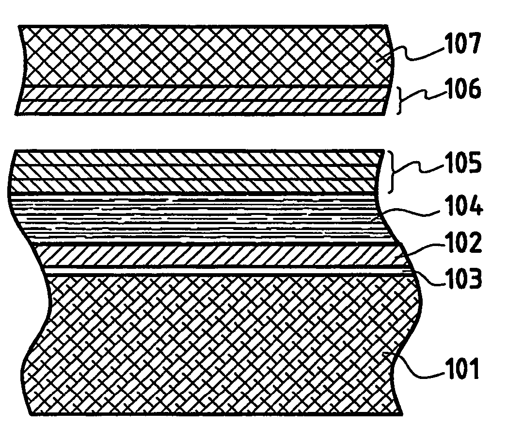
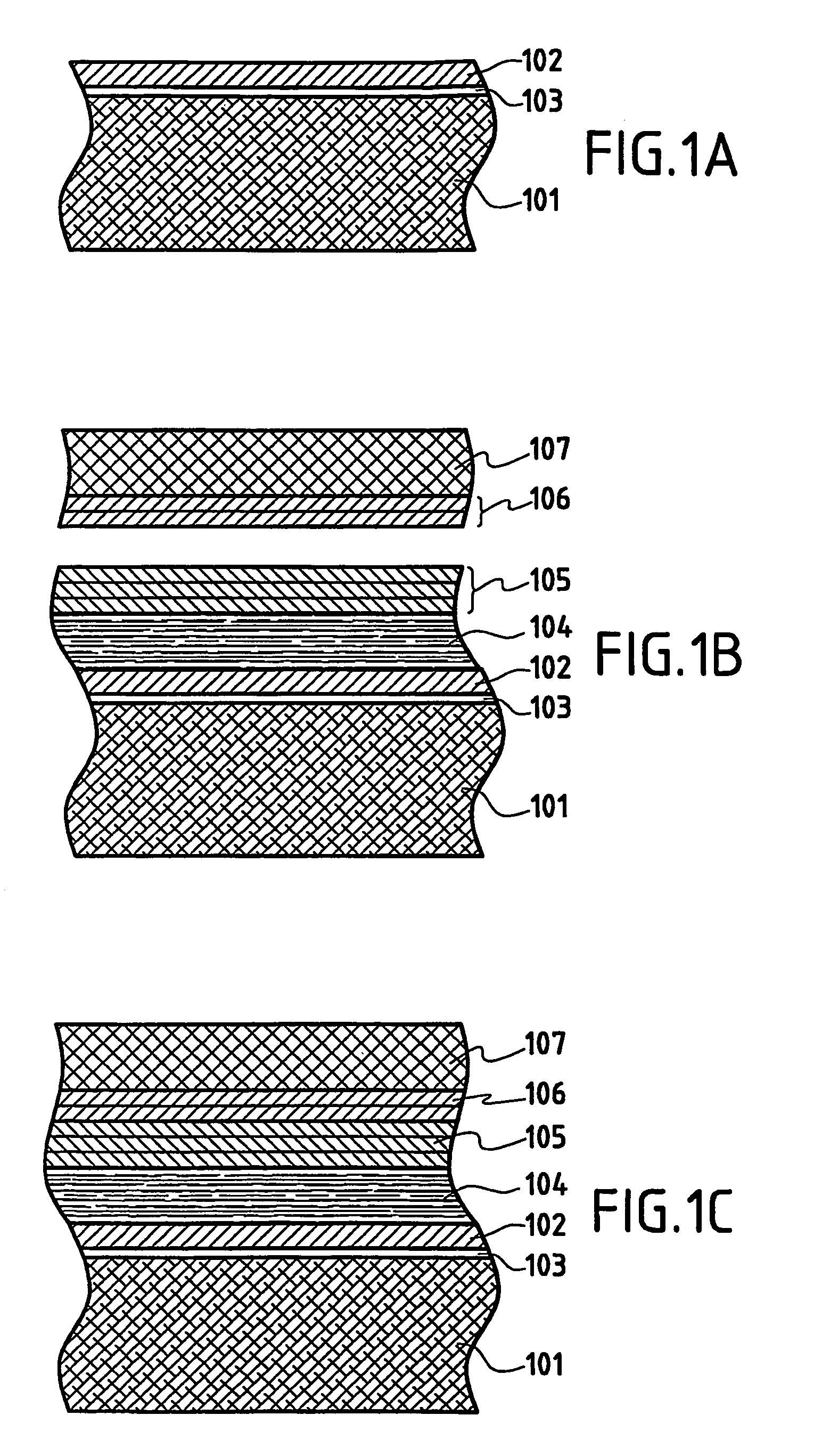
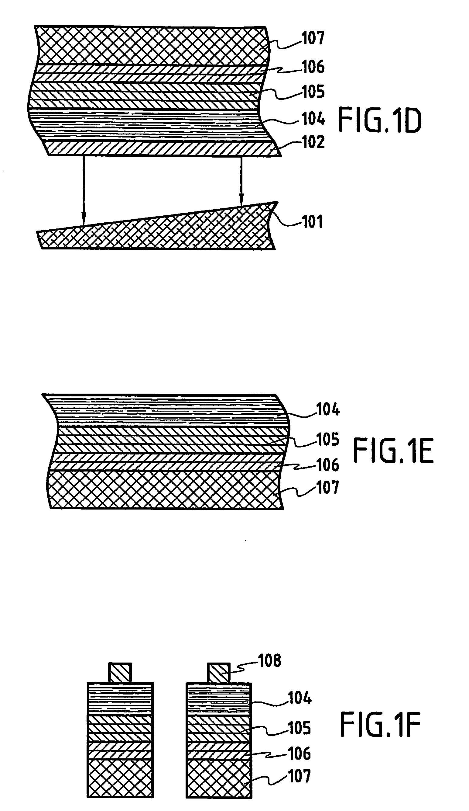
[0025] Metal bonding is preferably used to bond the transfer layer and the final substrate. Metal bonding is considered to be sufficiently strong mechanically and compatible with the subsequent step of separation at the weak interface without resulting in mechanical damage to the metal bonding interface and without destroying the initial support.

[0026] Metal bonding is advantageously achieved, for example, using a stack of layers comprising at least one ohmic contact layer formed directly on the epitaxially grown layer of semiconductor material, a reflective layer, and a layer based on gold or aluminum. The reflecting layer (mirror) is preferably based on silver, aluminum, rhodium, platinum, or gold. A supplemental layer can also be provided to act as a diffusion barrier, which can preferably be based on tungsten, titanium, chromium, platinum, or tantalum.

[0027] Metal bonding can be carried out using a metallic deposit formed on the transfer layer, the final substrate, or both. Th...


PUM

PropertyMeasurementUnit
thicknessaaaaaaaaaa
thicknessaaaaaaaaaa
thicknessaaaaaaaaaa

Abstract

Methods are provided for producing a transfer layer of a semiconductor material on a final substrate. In some embodiments, the transfer layer is produced on the final substrate by forming a layer of semiconductor material on an initial support, assembling that layer and a final substrate by metal bonding, and mechanically separating the initial support from the layer at a weak interface that initially attached the layer to the initial support. An intermediate substrate can be obtained which can be used to fabricate a variety of components such as light-emitting diodes or laser diodes. These techniques can produce a transfer layer on a final substrate and a recyclable initial support that can be detached from the transfer layer for recycling by a non-destructive mechanical release.

Description

CROSS-REFERENCE TO RELATED APPLICATIONS [0001] This application is a continuation of application Ser. No. 10 / 744,867 filed Dec. 22, 2003, the entire content of which is expressly incorporated herein by reference thereto.BACKGROUND [0002] The present invention relates to the field of assembling transfer layers and substrates. In particular, it is applicable to the production of light-emitting diodes (LEDs) or laser diodes (LDs) using layer transfer by metal bonding. [0003] The active layers of LEDs and LDs emitting in green, blue or ultraviolet (constituted, for example, by GaN or AlGaInN alloys) are usually grown epitaxially on sapphire or SiC substrates (see, for example, IEEE Journal On Selected Topics in Quantum Electronics, 8 (2002), 264, T. Mukai, “Recent progress in group-III nitride light emitting diodes”, or Phys. Stat. Sol. (a) 180 (2000) 5, V. Harle et al., “GaN-based LEDs and lasers on SiC”), while the active layers of LEDs or LDs emitting in the red, orange or yellow (co...

Claims


Application Information

Patent Timeline
Patent Type & Authority Applications(United States)
IPC IPC(8): H01L21/00H01L21/30H01L21/762H01L33/00
CPCH01L21/02032H01L21/76254H01L21/76259H01L33/0079H01L2924/0002H01L2924/00H01L33/0093
Inventor KERDILES, SEBASTIENLETERTRE, FABRICEMORALES, CHRISTOPHEMORICEAU, HUBERT
Owner SOITEC SA
Why Eureka
Try Eureka