Tri-state RF switch

Active Publication Date: 2006-10-12
SAMSUNG ELECTRONICS CO LTD
View PDF10 Cites 11 Cited by
  • Summary
  • Abstract
  • Description
  • Claims
  • Application Information

AI Technical Summary

Problems solved by technology

However, conventional RF switches only have one or two output signals for each input signal.
However, this configuration increases the complexity of the device.

Method used


Image

  • Tri-state RF switch
  • Tri-state RF switch
  • Tri-state RF switch

Examples


Embodiment Construction

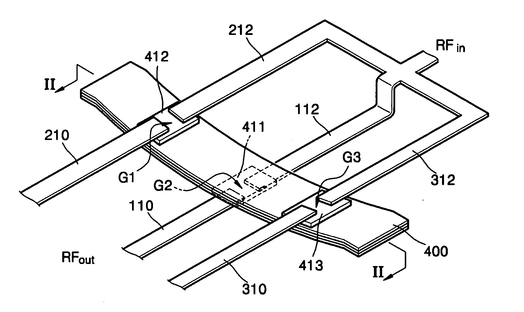
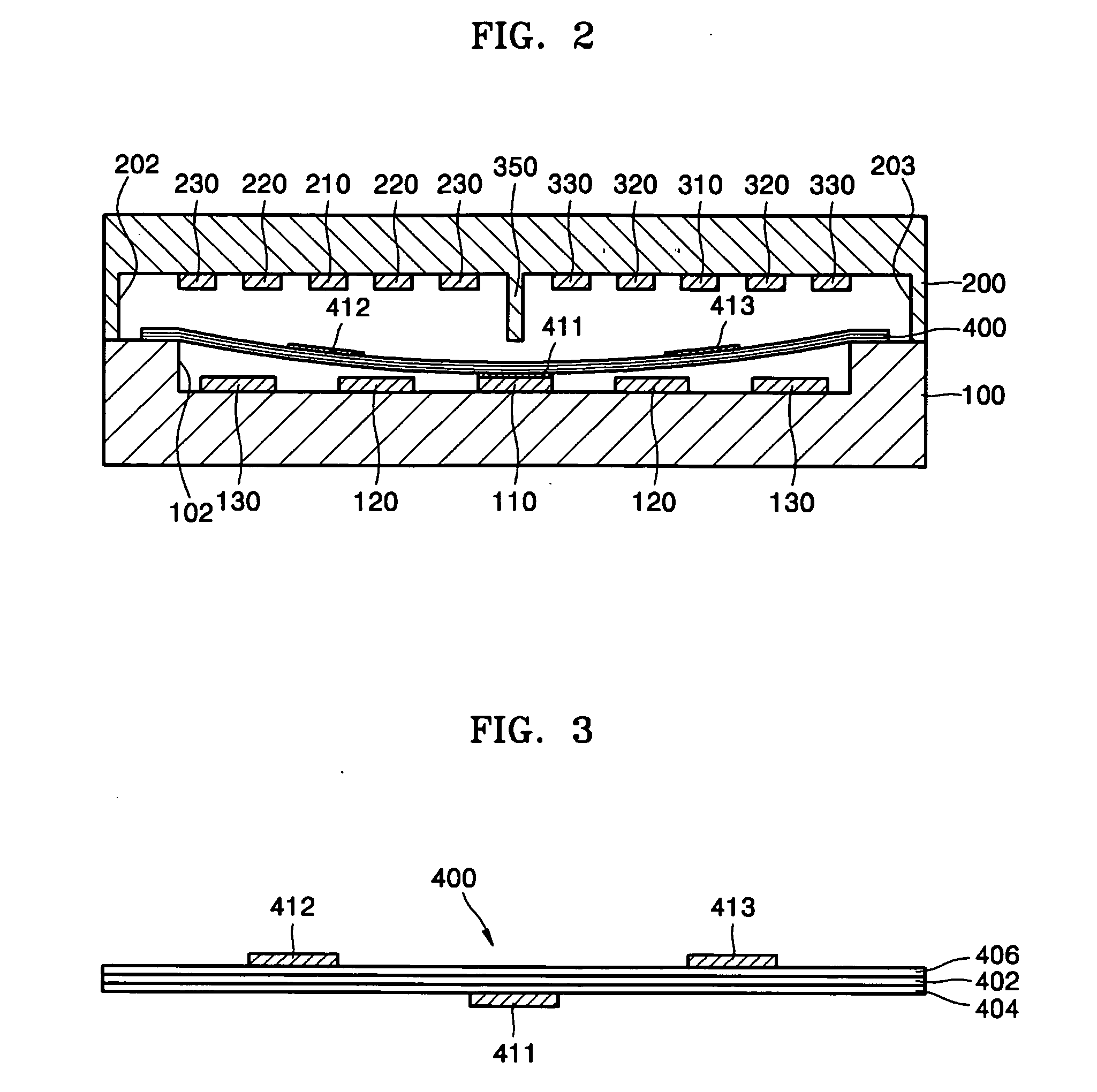
[0028]FIG. 1 is a schematic perspective view illustrating a structure of an RF switch according to an embodiment of the present invention. Referring to FIG. 1, an input signal line of an RF switch is divided into first through third input signal lines 112, 212, and 312, and first through third gaps G1, G2, and G3 are formed between the input signal lines 112, 212, and 312 and three output signal lines 110, 210, and 310. The first output signal line 110 and the second and third output signal lines 210 and 310 are located at different heights.

[0029] A membrane 400 that crosses the first through third gaps G1, G2, and G3 is formed between the first output signal line 110 and the two output signal lines 210 and 310. First through third conductive pads 411, 412, and 413 that correspond to first through third gaps G1, G2, and G3, respectively, are formed on the membrane 400, and the conductive pads 411, 412, and 413 can transfer electricity between corresponding input signal lines and ou...


PUM


Abstract

A tri-state RF MEMS switch includes: a first well formed in a first substrate; a first input signal line and a first output signal line forming a first gap therebetween in the first well; a post bar forming a boundary between the second well and third well in the second substrate; a second input signal line and a second output signal line, and a third input signal line and a third output signal line forming a second gap and a third gap in the second well and the third well, respectively; and a membrane disposed between the first substrate and the second substrate such that the membrane crosses the first, second and third gaps, the membrane including a first conductive pad, a second conductive pad, and a third conductive pad thereon to face the first, second and third gaps, respectively.

Description

CROSS-REFERENCE TO RELATED PATENT APPLICATIONS [0001] This application claims the benefit of Korean Patent Application No. 10-2005-0029575, filed on Apr. 8, 2005, in the Korean Intellectual Property Office, the disclosure of which incorporated herein in its entirety by reference. BACKGROUND OF THE INVENTION [0002] 1. Field of the Invention [0003] The present invention relates to a tri-state latching radio frequency (RF) switch and, more particularly, to an RF micro electromechanical system (MEMS) switch that is latched in one of three states (tri-states). [0004] 2. Description of the Related Art [0005] Radio frequency (RF) micro electromechanical system (MEMS) devices can be used in communications, radar, and WLAN technology. RF MEMS devices include micromachined capacitors, inductors, RF switches, phase shifters, tunable oscillators, etc. These devices have better characteristics than the devices manufactured by the prior art. For example, in comparison to a conventional FET or GaA...

Claims


Application Information

Patent Timeline
IPC IPC(8): H04B1/06
CPCH01H59/0009H01P1/127H01H2001/0042H01H59/00H01L29/00
Inventor CHOI, HYUNGJIAO, JIWEIWANG, YUELINXING, XIANGLONG
Owner SAMSUNG ELECTRONICS CO LTD
Why Eureka
Try Eureka