RF Switch with Integrated Tuning

a technology of integrated tuning and switch, which is applied in the direction of transmitter monitoring, transmission noise reduction, phase-modulated carrier system, etc., can solve the problems of increasing the complexity of radio frequency (rf) devices such as cell phone transmitters, increasing the number of components required in rf devices, increasing the complexity of routing the various components and increasing the cost associated with devices, so as to reduce the complexity of radio frequency (rf) circuital arrangemen

Active Publication Date: 2015-09-03
PSEMI CORP
View PDF3 Cites 59 Cited by
  • Summary
  • Abstract
  • Description
  • Claims
  • Application Information

AI Technical Summary

Benefits of technology

[0008]According to third aspect of the present disclosure a method for reducing complexity of a radio frequency (RF) circuital arrangement is presented, the method comprising: providing an RF switch comprising a common terminal and a plurality of switching terminals; providing an RF tuning circuit: coupling a first terminal of the RF tuning circuit to the common terminal of the RF switch; selecting, via the RF switch, an RF signal at a first switching terminal of the plurality of switching terminals of the RF switch; based on the selecting, configuring the RF tuning, circuit for at first tuning of a plurality of different tunings, and based on the selecting and the configuring, obtaining a tuned RF signal at a second port of the RF tuning circuit.

Problems solved by technology

Radio frequency (RF) devices, such as cell phone transmitters, are becoming increasingly complex due to additional frequency bands, more complex modulation schemes, higher modulation bandwidths, and the introduction of efficiency improvement schemes such as envelope tracking.
Such configuration can increase the number of components required in an RF device which in turn can increase the complexity of routing the various components as well as cost associated with the device.
Furthermore, with the usage of diversity antennas with the aim to reduce fading effects on a detected signal by building into the RF device redundant receive paths tuned to receive signals from the diversity antennas, more design and manufacturing challenges can be expected.

Method used


Image

  • RF Switch with Integrated Tuning
  • RF Switch with Integrated Tuning
  • RF Switch with Integrated Tuning

Examples


Embodiment Construction

[0020]Throughout this description, embodiments and variations are described for the purpose of illustrating uses and implementations of the inventive concept. The illustrative description should be understood as presenting examples of the inventive concept, rather than as limiting the scope of the concept as disclosed herein.

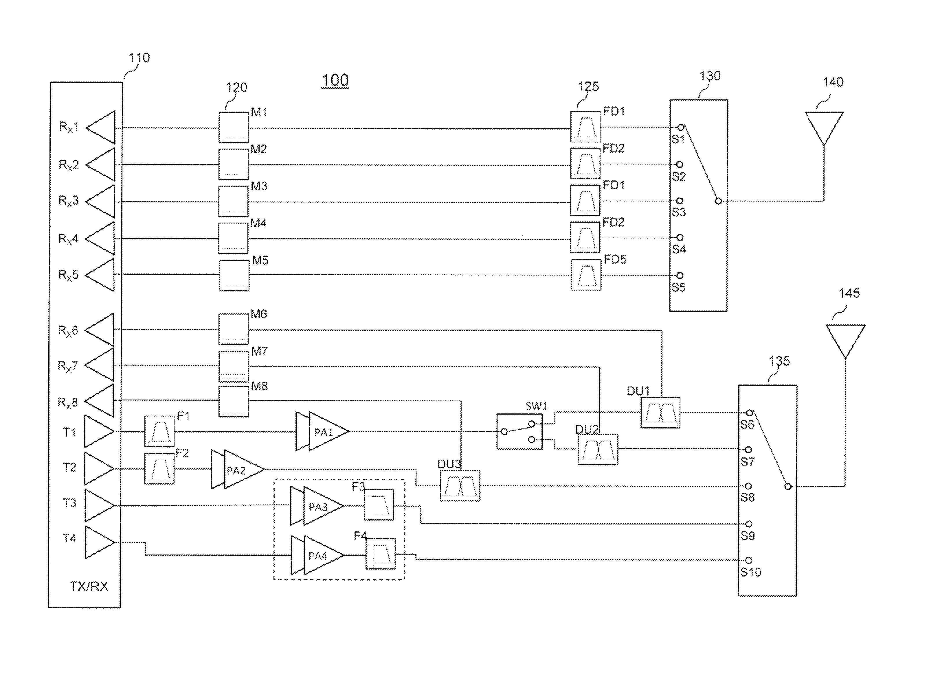
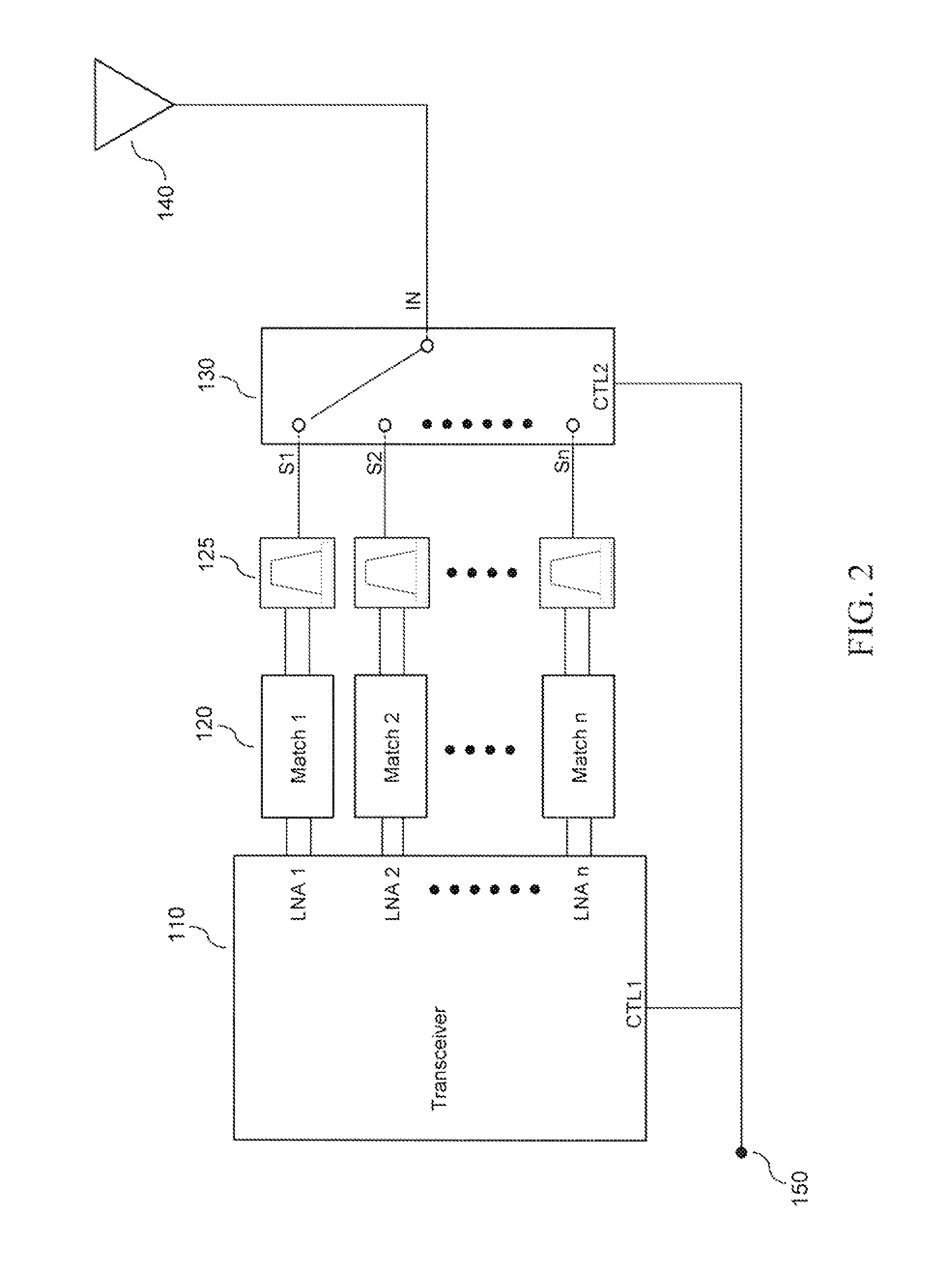
[0021]As used in the present disclosure, the terms “switch ON” and “activate” may be used interchangeably and can refer to making as particular circuit element electronically operational. As used in the present disclosure. the terms “switch OFF” and “deactivate” may be used interchangeably and can refer to making a particular circuit element electronically non-operational. As used in the present disclosure, the terms “amplifier” and “power amplifier” may be used interchangeably and can refer to a device that is configured to amplify a signal input to the device to produce an output signal of greater magnitude than the magnitude of the input signal.

[0022]The pres...


PUM


Abstract

Methods and devices are described for reducing receiver complexity in an RF front-end stage. In one exemplary implementation, a switch is used to connect a plurality of receive paths to a single input amplifier of a transceiver unit used the RF front-end stage. In another exemplary implementation, the switch has a tunable network which can be tuned with respect to various frequencies of operation of the receive path and associated RF signal.

Description

CROSS REFERENCE TO RELATED APPLICATIONS[0001]The present application may be related to U.S. Pat. No 6,804,502, issued on Oct. 12, 2004 and entitled “Switch Circuit and Method of Switching Radio Frequency Signals”, the disclosure of which is incorporated herein by reference in its entirety. The present application may also be related to U.S. Pat. No. 7,910,993, issued on Mar. 22, 2011 and entitled “Method and Apparatus for use in Improving Linearity of MOSFET's using an Accumulated Charge Sink”, the disclosure of which is incorporated herein by reference in its entirety. The present application may also be related to U.S. patent application Ser. No. 13 / 797,779 entitled “Sealable Periphery Tunable Matching Power Amplifier”, flied on Mar. 12, 2013, the disclosure of which is incorporated herein by reference in its entirety. The present application may also be related to International Application No. PCT / US2009 / 001358, entitled “Method and Apparatus for use in digitally tuning a capacit...

Claims


Application Information

Patent Timeline
Patent Type & Authority Applications(United States)
IPC IPC(8): H04B1/44H04B1/18H04B7/02
CPCH04B1/18H04B1/44H04B1/525H04B7/02H04B17/12H03F1/301H03F3/04H04B7/015H04B15/005H03F1/30H03F3/193H03F3/21H03F2200/451H03F2200/471H03F2200/555H03F3/195H03F3/213H03F2200/18H03F2200/456H04L27/20
Inventor NOBBE, DAN WILLIAM
Owner PSEMI CORP
Why Eureka
Try Eureka