

Optical identification chips
- Summary
- Abstract
- Description
- Claims
- Application Information
AI Technical Summary
Benefits of technology
Problems solved by technology
Method used
Image

Examples
Embodiment Construction
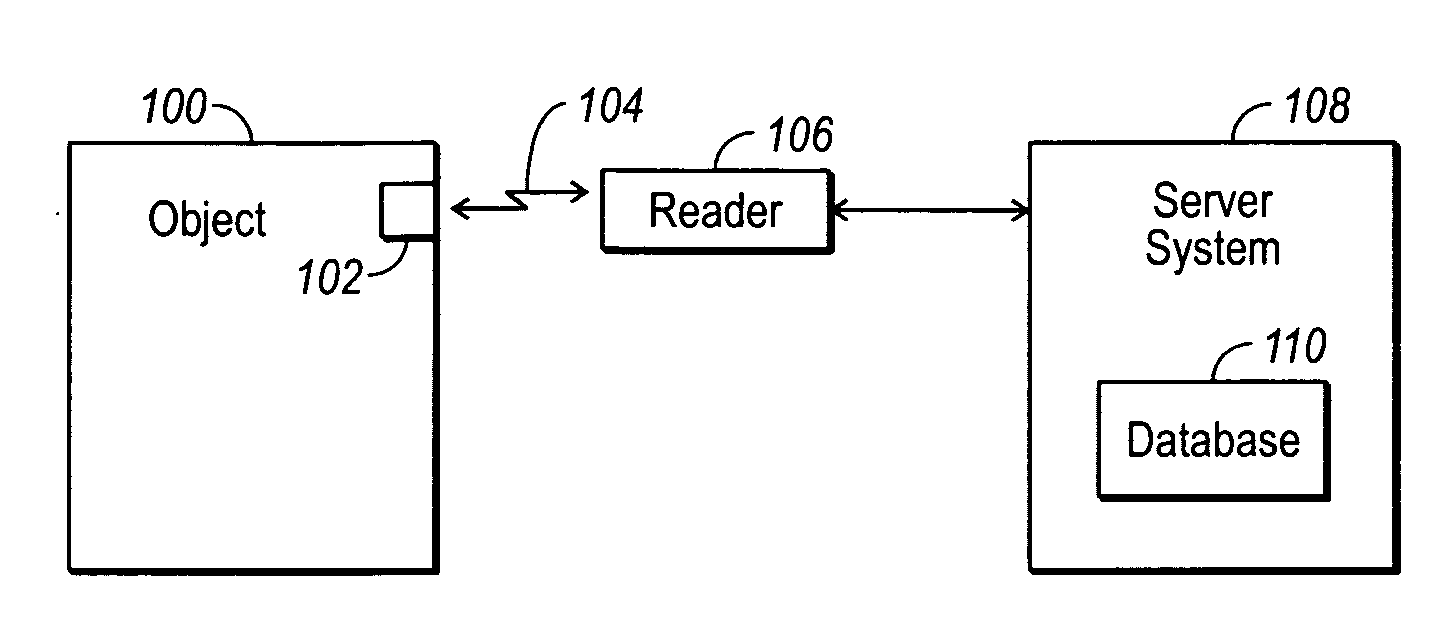
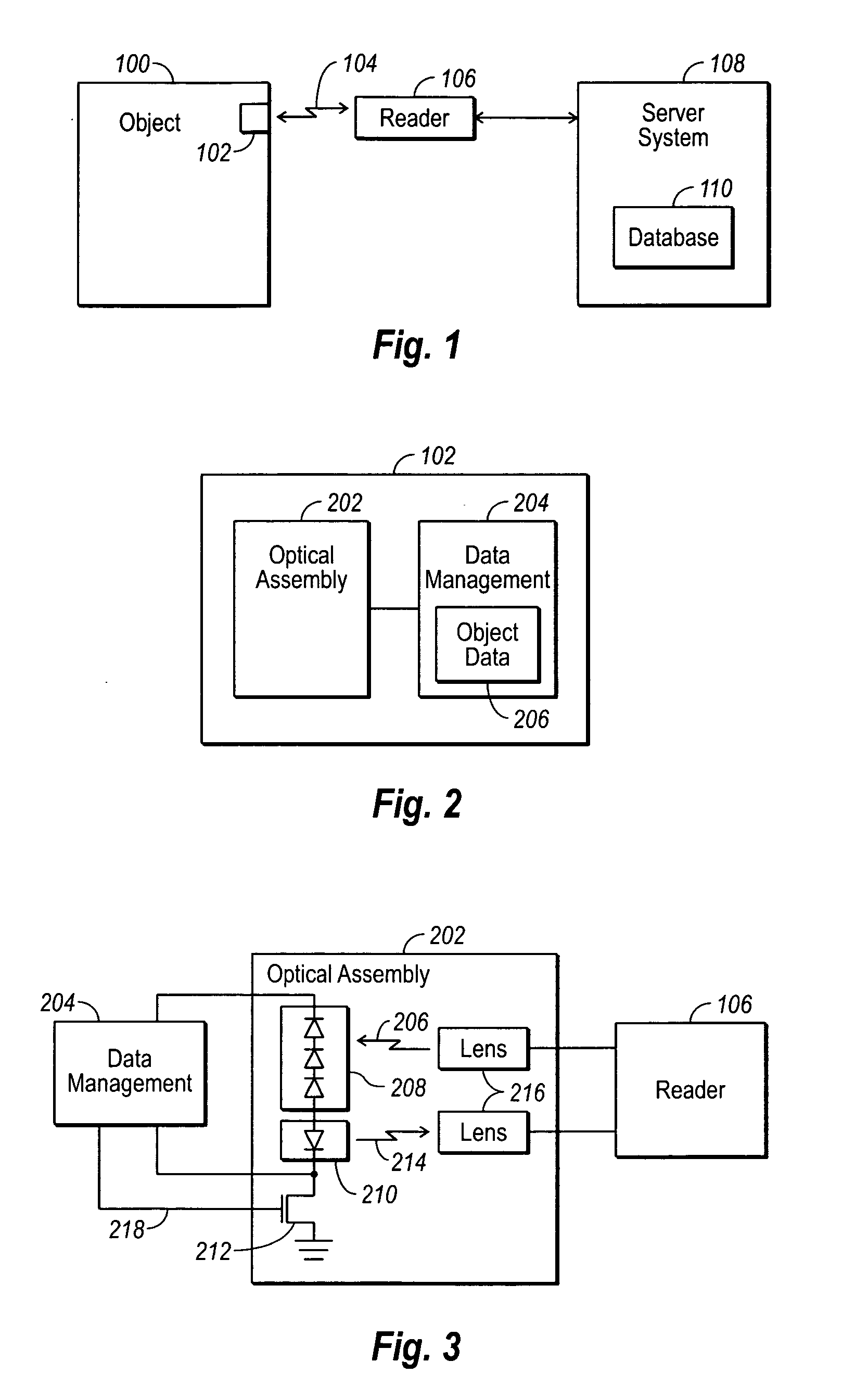
[0015] The present invention relates to identification devices that operate in the optical domain (e.g., in the visual or in the IR or other near-visual portions of the spectrum) and can be used to perform most of the functions conventionally performed by RFID systems, as well as be applied to new applications. The basic optical identification device includes two chips that are stacked together to form a single element. The resulting optical identification element (hereinafter “optical ID element”) can be as small as 1 mm3 or smaller, and as basic semiconductor processes continue to improve, can in the future be adapted to be much smaller.
[0016] One of the two chips is a pure complementary metal oxide semiconductor (CMOS) device that manages the identification information, receives data from incoming optical signals, and provides data that is to be encoded in outgoing optical signals. The CMOS chip interfaces with the other chip, which, in one embodiment, is an optical device that ...
PUM
 Abstract
Description
Claims
Application Information