Wirebonded device packages for semiconductor devices having elongated electrodes

Active Publication Date: 2006-11-09
INFINEON TECH AMERICAS
View PDF14 Cites 14 Cited by
  • Summary
  • Abstract
  • Description
  • Claims
  • Application Information

AI Technical Summary

Benefits of technology

[0015] According to an embodiment of the invention, a bond pad of a terminal lead intended to be connected to the elongated electrode is of an extended length and may extend parallel to and preferably adjacent to the elongated electrode. In addition, the bond pad may extend substantially along the full length of the electrode. In turn, a plurality of wirebonds are formed between the extended bond pad and elongated electrode. Notably, by configuring the bond pad in this fashion, the plurality of wirebonds between the electrode and bond pad may be spaced along the electrode and bond pad in a substantially parallel configuration and may have substantially equal lengths. Because of the substantially equal lengths, the plurality of wirebonds may have substantially the same resistance, thereby equalizing curre

Problems solved by technology

Significantly and as shown in FIG. 2, because the runners of the power electrodes of III-nitride based devices are elongated and because the bond pads of the terminal leads of conventional device packages are typically formed along the bottom of the package, the plurality of wirebonds between respective power electrodes and bond pads are long and of varying/unequal lengths, thereby making the device packages unsuitable.
Notably, the long length of the wirebonds increases package resistance, adds unwanted inductance, and also increases cost.
The length of the wirebonds also mak

Method used


Image

  • Wirebonded device packages for semiconductor devices having elongated electrodes
  • Wirebonded device packages for semiconductor devices having elongated electrodes
  • Wirebonded device packages for semiconductor devices having elongated electrodes

Examples


Embodiment Construction

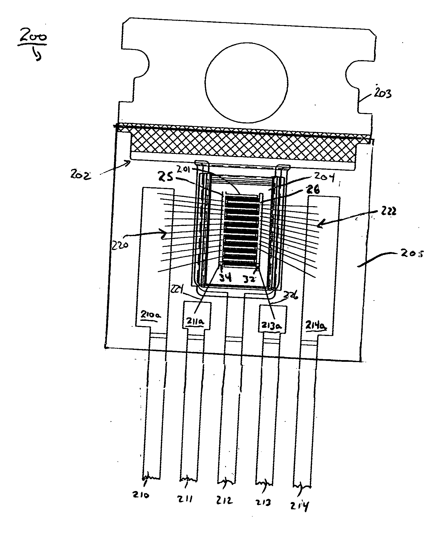
[0027] Referring to FIG. 3, there is shown a top plan view of a semiconductor device package 200 according to an embodiment of the invention. Device package 200 includes a lead frame 202 having a die pad 204 that is integral with a header 203, and further having a plurality of terminal leads, such as leads 210-214. As shown, one or more terminal leads, such as lead 212, may be integral with die pad 204. One skilled in the art will recognize that while device package 200 is shown as having a single die pad and five terminal leads, a device package according to this embodiment of the invention may have more than one die pad and may have more than or fewer than five terminal leads.

[0028] Device package 200 also includes at least one semiconductor device 201 mounted to die pad 204. Device 201 may be a III-nitride based power semiconductor device, such as a GaN-based device, that has one or more elongated electrodes and in particular, may be a unidirectional switch, a bi-directional swi...


PUM


Abstract

A device package includes at least one semiconductor device having at least one electrode of an elongated length. The device package also includes at least one conductive pad that extends parallel to the elongated length of the electrode. A terminal lead may be integral with the conductive pad. A plurality of wirebonds of about the same length may electrically connect the conductive pad and the elongated electrode of the semiconductor device. As another alternative, a second semiconductor device may be mounted to the conductive pad and a plurality of wirebonds may electrically connect this second device and the elongated electrode of the first semiconductor device.

Description

RELATED APPLICATIONS [0001] This application is based on and claims priority to U.S. Provisional Application No. 60 / 677,308, filed on May 3, 2005, by Glyn Connah, entitled, “WIREBONDED PACKAGE FOR GALLIUM NITRIDE BASED DEVICE,” the contents of which are herein incorporated by reference.BACKGROUND OF THE INVENTION [0002] 1. Field of the Invention [0003] This invention relates to semiconductor device packages and more specifically, relates to wirebonded semiconductor device packages having semiconductor devices that include elongated electrodes. [0004] 2. Description of the Art [0005] III-nitride based power semiconductor devices, such as Gallium Nitride (GaN) based devices, are desirable for power applications. Example III-nitride based devices include diodes, unidirectional switches, and bi-directional switches. These devices are lateral conductive devices with the power electrodes and control electrodes disposed along a top surface of the devices and with the bottom surface of the ...

Claims


Application Information

Patent Timeline
IPC IPC(8): H01L23/48
CPCH01L23/4824H01L2924/01033H01L23/5286H01L24/45H01L24/49H01L24/83H01L24/85H01L2224/0401H01L2224/45124H01L2224/45144H01L2224/48247H01L2224/49111H01L2224/49171H01L2224/83801H01L2224/85H01L2924/01013H01L2924/01014H01L2924/01027H01L2924/01028H01L2924/01031H01L2924/01079H01L2924/01082H01L2924/01083H01L2924/014H01L2924/30107H01L2224/04042H01L2224/05553H01L2224/48699H01L2224/48599H01L24/05H01L24/48H01L23/49562H01L2924/00014H01L2924/00H01L2924/00012H01L2924/10161
Inventor CONNAH, NORMAN GLYN
Owner INFINEON TECH AMERICAS
Why Eureka
Try Eureka