Pixel circuit, display device method for controlling pixel circuit

a display device and circuit technology, applied in static indicating devices, instruments, electroluminescent light sources, etc., can solve the problem of inability to disregarded power consumption of such devices, and achieve the effect of reducing luminance variation

Inactive Publication Date: 2006-11-16
SONY CORP
View PDF6 Cites 25 Cited by
  • Summary
  • Abstract
  • Description
  • Claims
  • Application Information

AI Technical Summary

Benefits of technology

[0048] As described above, as a method for reducing the variation of the luminance each in the pixel of the organic EL display, a pixel circuit by which the variation of property of each drive transistor determining a current for driving the organic EL element is corrected, has been proposed.
[0052] The present invention is to provide a pixel circuit and a display device capable of a low power consumption with the uniformity of luminance retained, and for realizing a high contrast and a high image quality, and a method for controlling the pixel circuit.

Problems solved by technology

Although the proposed pixel circuit retains a uniformity in luminance by setting the correction period in each frame in this way, and the circuit also performs a charge or discharge during the correction period, which causes the situation in which power consumption thereof may not able to be disregarded.

Method used


Image

  • Pixel circuit, display device method for controlling pixel circuit
  • Pixel circuit, display device method for controlling pixel circuit
  • Pixel circuit, display device method for controlling pixel circuit

Examples


first embodiment

[0095]FIG. 6 is a block diagram illustrating a configuration of an active matrix organic EL display (display device) employing a pixel circuit according to the first embodiment.

[0096]FIG. 7 is a circuit diagram illustrating a basic configuration of the pixel circuit in the organic EL display shown in FIG. 6.

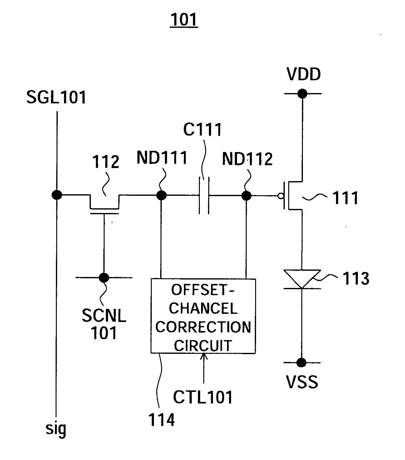
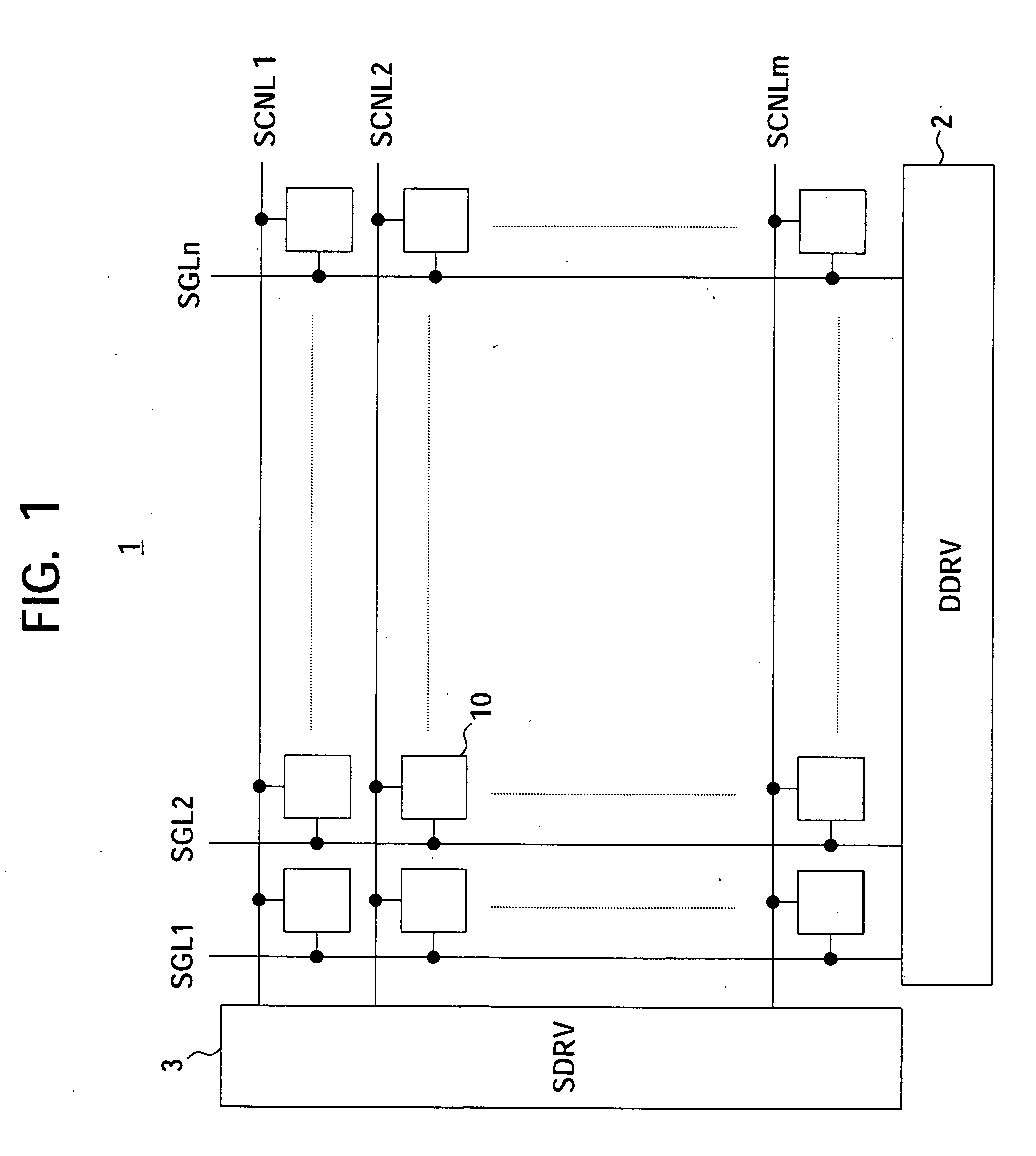
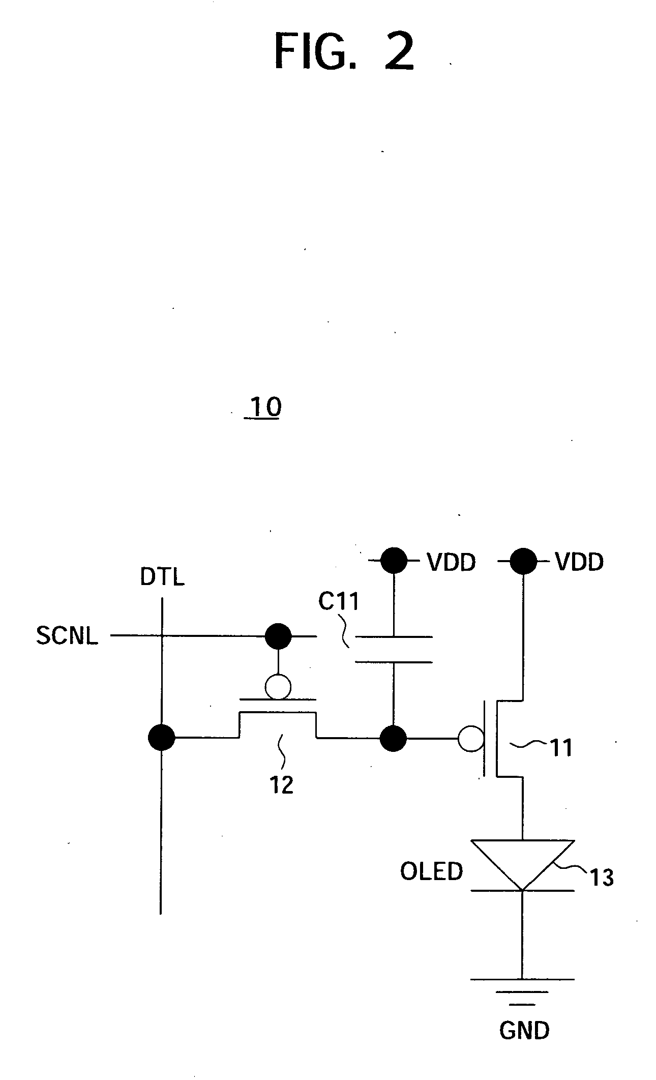
[0097] An organic EL display 100 has a pixel array portion 102 including pixel circuits 101 arranged in an m×n matrix, a data driver (DDRV) 103, and a scan driver (SDRV) 104.

[0098] With respect to the matrix arrangement of the pixel circuit 101, the n number of column's worth of signal lines SGL101-1 to SGL101-n selected and driven by the data driver (DDRV) 103 is interconnected in each pixel row, and the m number of row's worth of scan lines SCNL101-1 to SCNL101-m as first control lines and the m number of row's worth of offset-chancel correction control lines CTL101-1 to CTL101-m as second control lines, which are selected and driven by the scan driver (SDRV) 104, are interc...

second embodiment

[0119]FIG. 10 is a block diagram illustrating a configuration of an active matrix organic EL display (display device) employing a pixel circuit according to a second embodiment.

[0120]FIGS. 11A to 11C are views for illustrating a second drive control method of the entire pixel array portion of an organic EL display 100A having pixel circuits in which an offset-chancel correction in the second embodiment is performed.

[0121]FIG. 12 is a timing chart for illustrating the second drive control method of the entire pixel array portion of the organic EL display 100A having the pixel circuits in which the offset-chancel correction in the second embodiment is performed.

[0122] The components of the pixel circuit 101 in the second embodiment are the same as those of the first embodiment.

[0123] A different point of the second embodiment from the above first embodiment resides in that, in the offset-chancel correction, the scan driver 104A changes drive control lines CTL101-1 to CTL101-m in e...

third embodiment

[0129]FIG. 13 is a block diagram illustrating a configuration of an active matrix organic EL display (display device) employing a pixel circuit according to the third embodiment.

[0130]FIGS. 14A to 14C are views for illustrating a third drive control method of the entire pixel array portion 102 of the organic EL display 100B having the pixel circuits in which an offset-chancel correction in the third embodiment is performed.

[0131]FIG. 15 is a timing chart illustrating the third drive control method of the entire pixel array portion 102 of the organic EL display 100B having the pixel circuits in which the offset-chancel correction in the third embodiment is performed.

[0132] The components of the pixel circuit 101 in the third embodiment are the same as those of the first and second embodiments.

[0133] A different point of the third embodiment from the above second embodiment resides in that first correction control lines CTL101-1 to 101-m and second correction control lines 102-1 t...


PUM


Abstract

A pixel electrode and a display device capable of lowering a power consumption with a uniformity of a luminance retained, and realizing a display image having a high contrast and a high image quality, wherein a correction period for correcting a variation of property of a drive transistor in a pixel during a frame, a write period for driving a first switch by a first control line and writing a data signal from a signal line to the node, and a drive period for storing the written data signal and driving a electro-optical element, are set, and the drive is controlled so that an interval having the correction period, the write period, and the drive period, and an interval having the write period and the drive period without the correction period exist.

Description

CROSS REFERENCES TO RELATED APPLICATIONS [0001] The present invention contains subject matter related to Japanese Patent Application No. 2005-139898 filed in the Japanese Patent Office on May 12, 2005, the entire contents of which being incorporated herein by reference. BACKGROUND OF THE INVENTION [0002] 1. Field of the Invention [0003] The present invention relates to a pixel circuit having an electro-optical element in which a luminance is controlled by a signal line, a display device, such as an organic EL (electroluminescence) display, a LCD (liquid crystal display) device, or other active matrix display device, in which a plurality of the pixel circuit is arranged in matrix, and a method for controlling the pixel circuit. [0004] 2. Description of the Related Art [0005] In the active matrix display device, a liquid crystal cell, an organic EL element, or other electro-optical elements is used as a display element in a pixel. [0006] Among them, the organic EL element has a struct...

Claims


Application Information

Patent Timeline
Patent Type & Authority Applications(United States)
IPC IPC(8): G09G3/36H05B44/00
CPCG09G3/3233G09G2300/0417G09G2300/0819G09G2320/043G09G2300/0852G09G2300/0861G09G2310/0262G09G2300/0842G09G3/30G09G3/20
Inventor ASANO, MITSURUYUMOTO, AKIRAFUJIMURA, HIROSHI
Owner SONY CORP
Why Eureka
Try Eureka