Intelligent system for detection of process status, process fault and preventive maintenance

Inactive Publication Date: 2006-11-16
TOKYO ELECTRON LTD
View PDF11 Cites 46 Cited by
  • Summary
  • Abstract
  • Description
  • Claims
  • Application Information

AI Technical Summary

Problems solved by technology

However, processing conditions can change over time, with small ch

Method used


Image

  • Intelligent system for detection of process status, process fault and preventive maintenance
  • Intelligent system for detection of process status, process fault and preventive maintenance
  • Intelligent system for detection of process status, process fault and preventive maintenance

Examples


Embodiment Construction

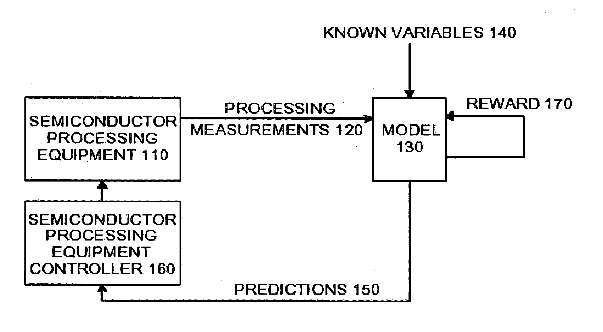
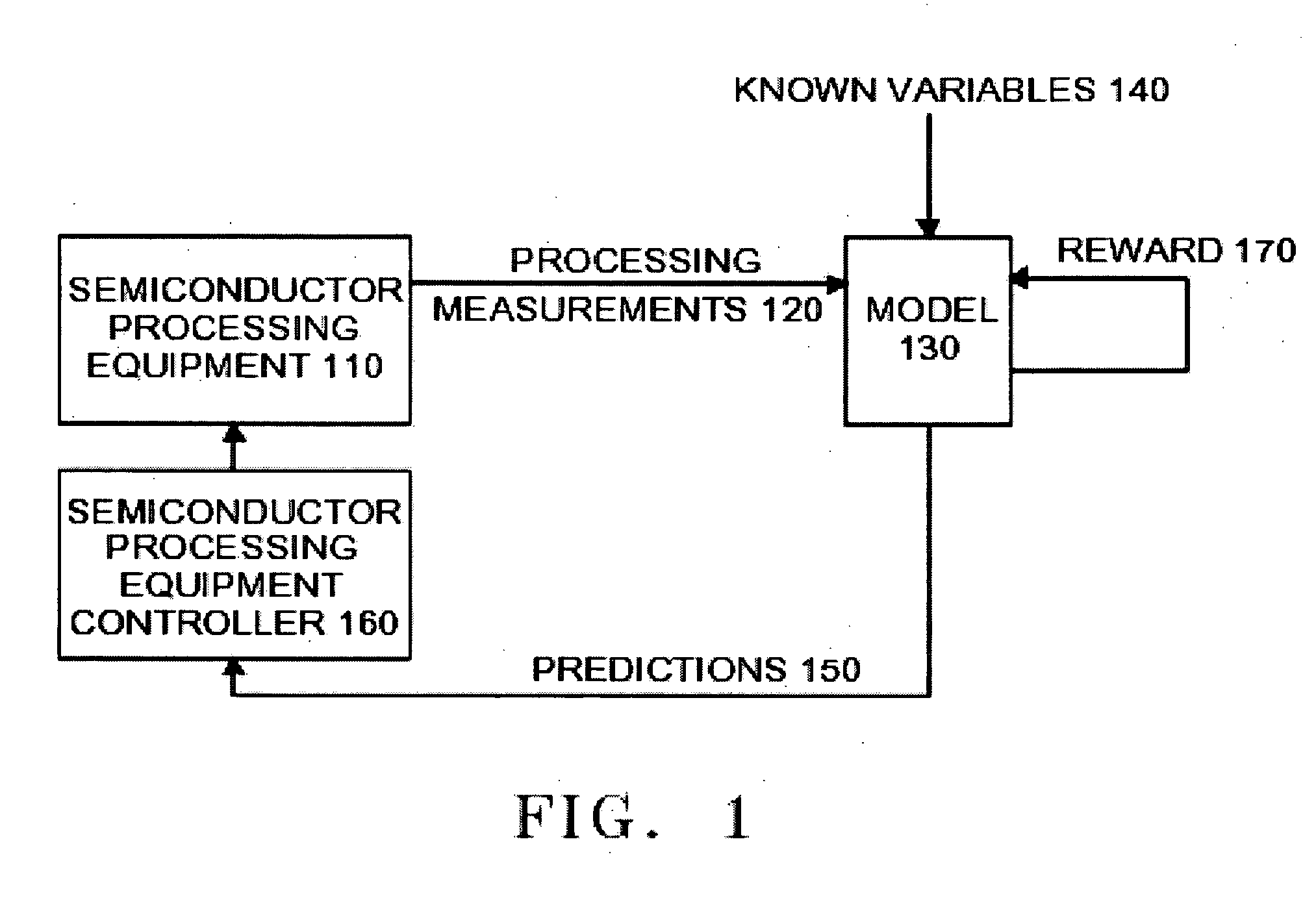
[0012] Various embodiments of the present invention are directed to intelligent modeling methods and systems that monitor and perform analysis of semiconductor processing equipment as well as predict future states of that equipment based on the analysis, predict failures of the semiconductor processing equipment and / or determine equipment maintenance schedules.

[0013] Accordingly, the system model may obtain data indicating process measurements and known variables, for example, the time or times of last cleaning or maintenance or the time or times of last failures, to predict failure, next cleaning, and / or preventative maintenance schedules.

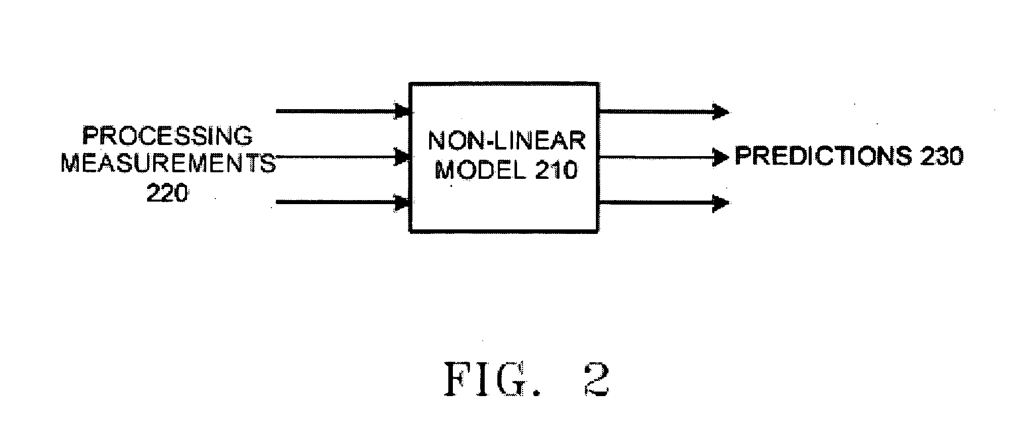
[0014]FIG. 1 illustrates a reinforcement learning system 100 whereby semiconductor processing equipment 110 outputs various process measurements 120, such as chamber temperature, gas mixture and applied Radio Frequency (RF) power, which are input into the model 130. Known variables 140, such as the time between a last equipment cleaning interval...


PUM


Abstract

Embodiments of an intelligent modeling method and system monitor and perform analysis of semiconductor processing equipment as well as predict future states of that equipment based on the analysis, predict failures of the semiconductor processing equipment and/or determine equipment maintenance schedules.

Description

[0001] This is a Continuation application of International Patent Application No. PCT / US04 / 036499, filed on Nov. 3, 2004, which relies for priority on U.S. Provisional Patent Application No. 60 / 524,846, filed Nov. 26, 2003, the entire contents of both of which are incorporated herein by reference in their entireties.FIELD OF THE INVENTION [0002] The present invention relates to control systems, particularly to a system in a semiconductor processing facility designed to monitor performance, predict failures and determine maintenance schedules. BACKGROUND OF THE INVENTION [0003] Semiconductor processing techniques represent complex, non-linear physical environments wherein various process variables are under the control of an operator. Indeed, typically, an operator is in control of ten or more process variables that require constant monitoring. However, processing conditions can change over time, with small changes in critical process parameters creating undesirable results. These ch...

Claims


Application Information

Patent Timeline
IPC IPC(8): G05B19/04G05B19/418G05B23/02
CPCG05B19/4184G05B23/0254G05B2219/24019G05B2219/45031G05B2219/32234G05B2219/33296G05B2219/31357Y02P90/02Y02P90/80
Inventor BRCKA, JOZEFDELP, DEANAGRAPPERHAUS, MICHAELMOROZ, PAUL
Owner TOKYO ELECTRON LTD
Why Eureka
Try Eureka