
Eureka
For R&D, Eureka makes reading and utilizing patents & technical documents easy.
Eureka AIR
Designed for self-driven R&D workflows. Generate viable solutions, solve complex R&D challenges, empower your innovation with AI.

Eureka Materials
Designed for material experts only. Revolutionize your material R&D, from search, analyze, to developing new materials.

TechResearch
Generate reliable direction feasibility study reports for your R&D in just a few steps.

TechSeek
Discover and master advanced knowledge NOW. Basics, ideas, possibilities, all at once.

TechMind
As an expert in R&D Theories, TechMind can generates customized viable solutions instantly.

TechRisk
Analyze your overall solution with one click, know your potential R&D risks in advance.

TechMonitor
Get weekly tech updates, stay abreast of the latest tech innovations and key insights.
Apparatus and method for inspecting a wafer
- Summary
- Abstract
- Description
- Claims
- Application Information
AI Technical Summary
Benefits of technology
Problems solved by technology
Method used
Image

Examples
Embodiment Construction
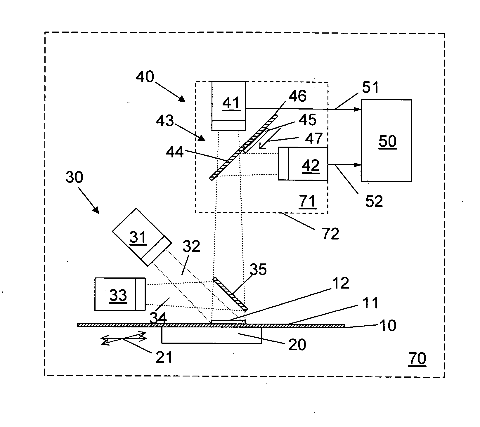
[0038]FIG. 1, in a schematic representation, shows the apparatus of the present invention comprising the movement means 20, the illumination means 30, the imaging means 40 and the evaluation means 50.
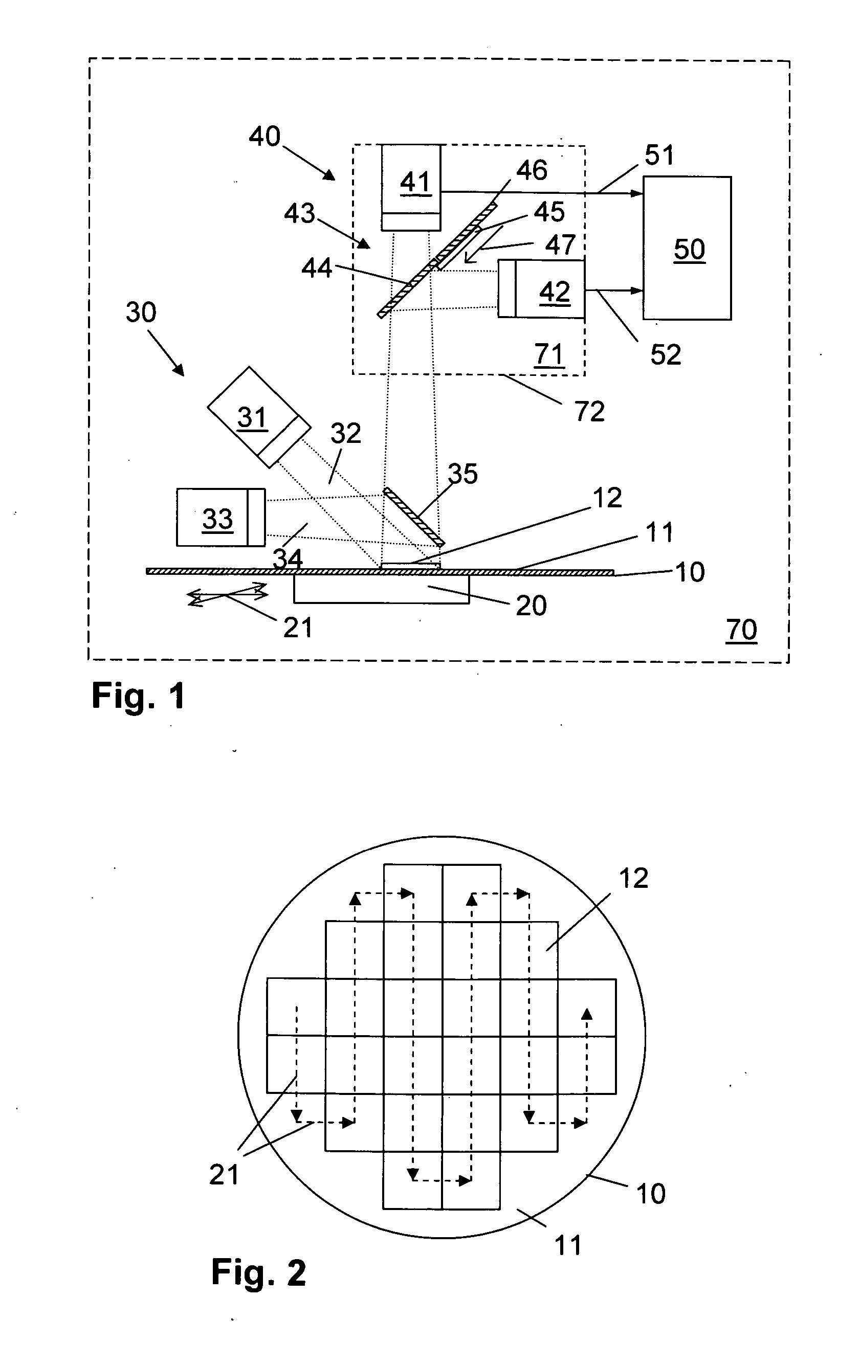
[0039] The wafer 10 is supported by a movement means 20 which can transport the wafer in the movement direction 21. An imaging area 12 is shown on the wafer surface 11. This imaging area 12 is illuminated by the illumination means 30. The illumination means 30 comprises a dark-field light source 31 and a bright-field light source 33, as well as a beam splitting mirror 35. The dark-field light source 31, with its illumination beam 32, illuminates the imaging area 12 at an angle. The light beam 34 of the bright-field light source 33 is projected by a beam splitting mirror 35 in parallel to the imaging beam path.
[0040] The imaging means 40 comprises a color camera 41, a black and white camera 42 and an image allocation optics 43. The image allocation optics 43 consists of a first beam sp...
PUM
 Abstract
Description
Claims
Application Information
 - R&D Engineer
- R&D Manager
- IP Professional
- Industry Leading Data Capabilities
- Powerful AI technology
- Patent DNA Extraction
Browse by: Latest US Patents, China's latest patents, Technical Efficacy Thesaurus, Application Domain, Technology Topic, Popular Technical Reports.
© 2024 PatSnap. All rights reserved.Legal|Privacy policy|Modern Slavery Act Transparency Statement|Sitemap|About US| Contact US: help@patsnap.com