Multi-test method for using compare MISR

a compare misr and multi-testing technology, applied in error detection/correction, instruments, computing, etc., can solve the problem of reducing the bandwidth required to communicate the result(s), and achieve the effect of reducing the number of pins/connections and reducing the amount of processing

Inactive Publication Date: 2006-12-14
KK TOSHIBA
View PDF30 Cites 40 Cited by
  • Summary
  • Abstract
  • Description
  • Claims
  • Application Information

AI Technical Summary

Benefits of technology

[0013] One or more of the problems outlined above may be solved by the various embodiments of the invention. Broadly speaking, the invention includes systems and methods for performing logic built-in-self-tests...

Problems solved by technology

This single bit result reduces the bandwidth required to com...

Method used


Image

  • Multi-test method for using compare MISR
  • Multi-test method for using compare MISR
  • Multi-test method for using compare MISR

Examples


Embodiment Construction

[0030] One or more embodiments of the invention are described below. It should be noted that these and any other embodiments described below are exemplary and are intended to be illustrative of the invention rather than limiting.

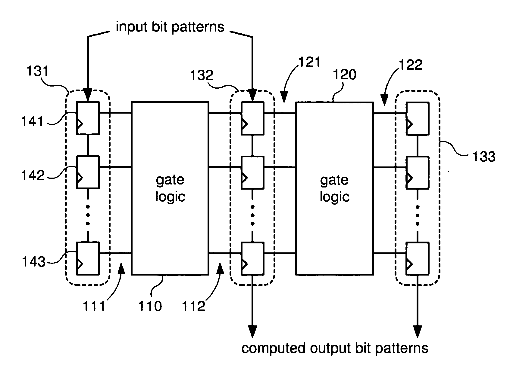
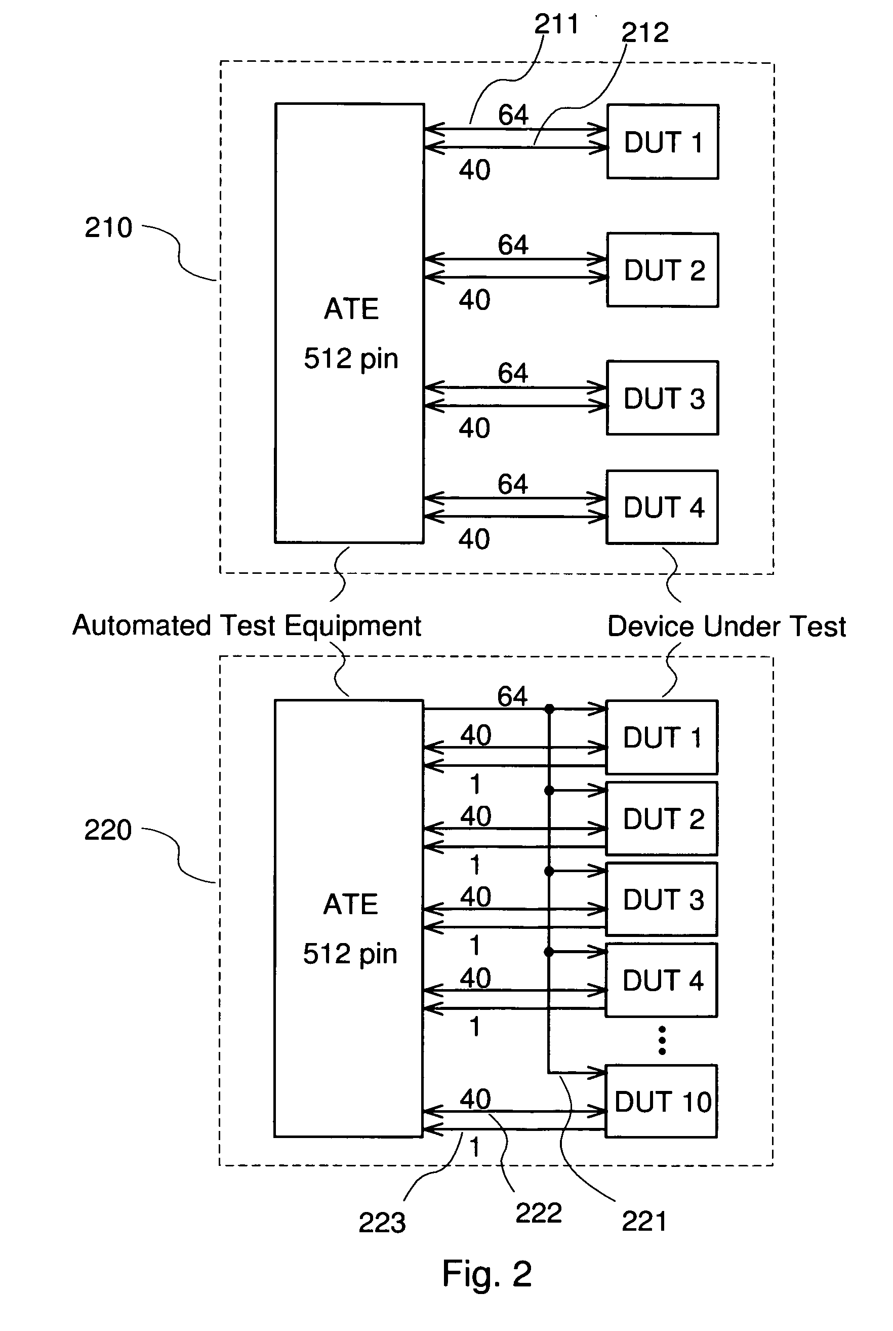
[0031] Broadly speaking, the invention includes systems and methods for increasing the number of devices having LBIST circuitry that can be tested at the same time by reducing the number of necessary connections between the devices under test and a test system. Various embodiments may reduce the bandwidth required of the logic built-in-self-test (LBIST) circuitry and increase the number of devices that can be connected automated test equipment when performing logic built-in-self-tests. These benefits can be obtained by configuring the LBIST circuitry to perform evaluations of computed results within the same device (“on-chip”).

[0032] In one embodiment, a STUMPS-type LBIST test architecture is incorporated into the design of a logic circuit. The LBIST compo...


PUM


Abstract

Systems and methods for performing logic built-in-self-tests (LBISTs) where data comparisons are performed in the MISR. In one embodiment, a STUMPS-type LBIST architecture includes scan chains interposed between portions of the functional logic of the logic circuit. Test bit patterns are scanned into the scan chains, propagated through the functional logic, and captured in scan chains following the functional logic. The bits are scanned out of the scan chains into a self-compare MISR that creates a signature from the computed bit patterns and then compares the signature of the computed bit patterns with an expected signature, giving a pass/fail result. This single bit result reduces the bandwidth required to communicate the result(s) of the LBIST testing to the test equipment. As a result, a larger number of devices can be tested by a given piece of test equipment.

Description

BACKGROUND [0001] 1. Field of the Invention [0002] The invention relates generally to the testing of electronic circuits, and more particularly to systems and methods for increasing the number of devices having LBIST circuitry that can be tested at the same time by reducing the number of necessary connections between the devices under test and a test system. [0003] 2. Related Art [0004] Digital devices are becoming increasingly complex. As the complexity of these devices increases, there are more and more chances for defects that may impair or impede proper operation of the devices. The testing of these devices is therefore becoming increasingly important. [0005] Testing of a device may be important at various stages, including in the design of the device, in the manufacturing of the device, and in the operation of the device. Testing at the design stage ensures that the design is conceptually sound. Testing during the manufacturing stage may be performed to ensure that the timing, ...

Claims


Application Information

Patent Timeline
IPC IPC(8): G01R31/28G06F11/00
CPCG01R31/318563G01R31/318547
Inventor KIRYU, NAOKI
Owner KK TOSHIBA
Why Eureka
Try Eureka