Method and system for driving a light emitting device display

a technology of light-emitting devices and displays, applied in the field of display technologies, can solve the problems of controlling signals, high power consumption, and inability to adopt a time-based display schedule in large-area displays

Active Publication Date: 2006-12-28
IGNIS INNOVATION
View PDF39 Cites 139 Cited by
  • Summary
  • Abstract
  • Description
  • Claims
  • Application Information

AI Technical Summary

Benefits of technology

[0007] It is an object of the invention to provide a method and system that obviates or mitigates at least one of the disadvantages of existing systems.

Problems solved by technology

However, since the VT-generation cycle “VT-GEN” requires a large timing budget to generate an accurate threshold voltage of a drive TFT, this timing schedule cannot be adopted in large-area displays.
Moreover, executing two extra operating cycles (i.e., “C” and “VT-GEN”) results in higher power consumption and also requires extra controlling signals leading to higher implementation cost.

Method used


Image

  • Method and system for driving a light emitting device display
  • Method and system for driving a light emitting device display
  • Method and system for driving a light emitting device display

Examples


Embodiment Construction

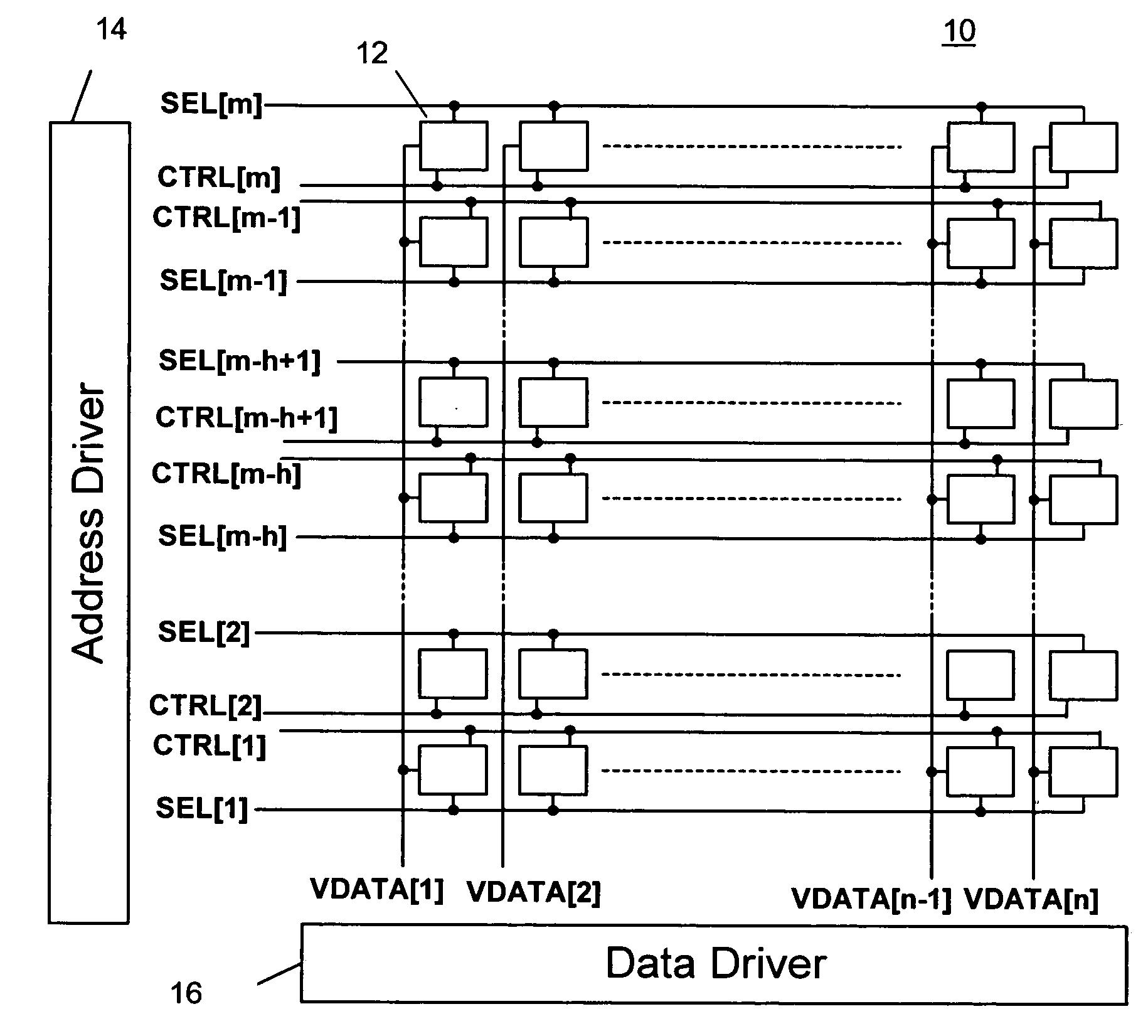
[0036] Embodiments of the present invention are described using a pixel circuit having a light emitting device, such as an organic light emitting diode (OLED), and a plurality of transistors, such as thin film transistors (TFTs), arranged in row and column, which form an AMOLED display. The pixel circuit may include a pixel driver for OLED. However, the pixel may include any light emitting device other than OLED, and the pixel may include any transistors other than TFTs. The transistors in the pixel circuit may be n-type transistors, p-type transistors or combinations thereof. The transistors in the pixel may be fabricated using amorphous silicon, nano / micro crystalline silicon, poly silicon, organic semiconductors technologies (e.g. organic TFT), NMOS / PMOS technology or CMOS technology (e.g. MOSFET). In the description, “pixel circuit” and “pixel” may be used interchangeably. The pixel circuit may be a current-programmed pixel or a voltage-programmed pixel. In the description below...


PUM


Abstract

A method and system for driving a light emitting device display is provided. The system provides a timing schedule which increases accuracy in the display. The system may provide the timing schedule by which an operation cycle is implemented consecutively in a group of rows. The system may provide the timing schedule by which an aging factor is used for a plurality of frames.

Description

FIELD OF INVENTION [0001] The present invention relates to display technologies, more specifically a method and system for driving light emitting device displays. BACKGROUND OF THE INVENTION [0002] Recently active-matrix organic light-emitting diode (AMOLED) displays with amorphous silicon (a-Si), poly-silicon, organic, or other driving backplane have become more attractive due to advantages over active matrix liquid crystal displays. An AMOLED display using a-Si backplanes, for example, has the advantages that include low temperature fabrication that broadens the use of different substrates and makes flexible displays feasible, and its low cost fabrication. Also, OLED yields high resolution displays with a wide viewing angle. [0003] The AMOLED display includes an array of rows and columns of pixels, each having an organic light-emitting diode (OLED) and backplane electronics arranged in the array of rows and columns. Since the OLED is a current driven device, the pixel circuit of t...

Claims


Application Information

Patent Timeline
Patent Type & Authority Applications(United States)
IPC IPC(8): G09G3/30
CPCG09G3/3233G09G3/3258G09G2300/043G09G2300/0819G09G2300/0842G09G2300/0852G09G2320/0233G09G2310/0218G09G2310/0221G09G2310/0283G09G2320/043G09G2320/045G09G2330/021G09G2310/0216G09G3/20G09G3/30G09G3/32H05B33/12
Inventor NATHAN, AROKIACHAJI, G. REZA
Owner IGNIS INNOVATION
Why Eureka
Try Eureka