Picture processing apparatus, semiconductor integrated circuit, and method for controlling a picture memory

a picture memory and processing apparatus technology, applied in the direction of memory adressing/allocation/relocation, color signal processing circuits, television systems, etc., can solve the problems of overhead cycles (cycles other than accessing data) and the inability to realize high-speed memory access

Inactive Publication Date: 2006-12-28
KK TOSHIBA
View PDF1 Cites 5 Cited by
  • Summary
  • Abstract
  • Description
  • Claims
  • Application Information

AI Technical Summary

Problems solved by technology

On the other hand, when pages within the same bank are switched, overhead cycles (cycles other than accessing data) increase.
However, in the abovementioned techniq

Method used


Image

  • Picture processing apparatus, semiconductor integrated circuit, and method for controlling a picture memory
  • Picture processing apparatus, semiconductor integrated circuit, and method for controlling a picture memory
  • Picture processing apparatus, semiconductor integrated circuit, and method for controlling a picture memory

Examples


first modification

(First Modification)

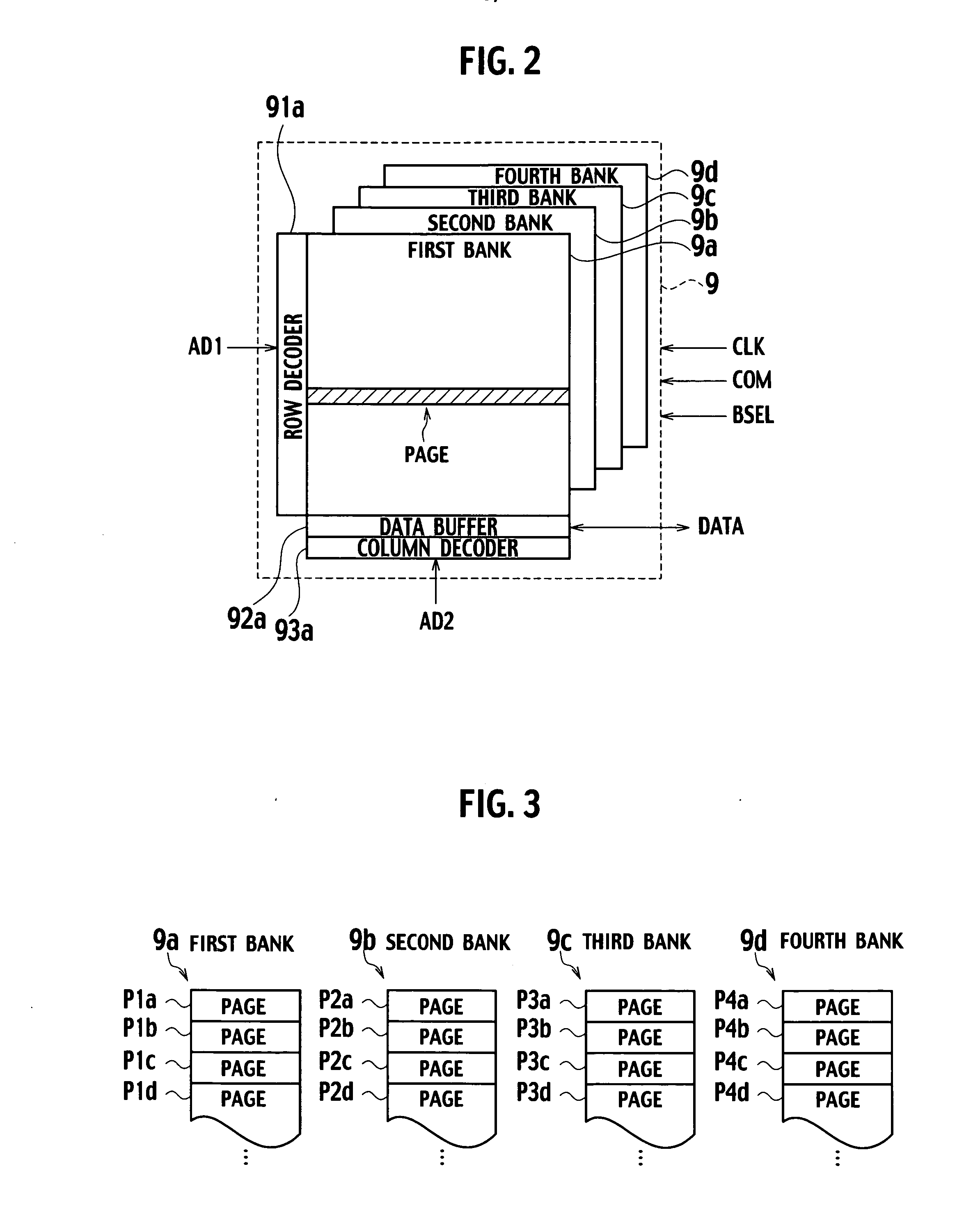
[0082] It is acceptable to establish the picture memory 9 with a count of 8 banks as the picture processing apparatus according to the first modification of the embodiment of the present invention. Further, it is acceptable for each page to have a memory capacity of 4096 bytes as shown in FIG. 20. As a result, the number of pixels in the horizontal direction of each page is 128, and 4 of the storage regions of the picture data of the pixels occupying the even and odd lines are disposed in the horizontal direction, in the virtual two-dimensional memory region. Other arrangements are similar to those of FIG. 7 and FIG. 8. According to the first modification of the embodiment of the present invention, it is possible to use the picture memory 9 having an 8 bank structure wherein the memory capacity of each page is 4096 bytes.

second modification

(Second Modification)

[0083] It is acceptable to establish the picture memory 9 with a count of 8 banks as the picture processing apparatus according to the second modification of the embodiment of the present invention. Further, it is acceptable for each page to have a data storage capacity of 4096 bytes, as shown in FIG. 21. However, the point of the picture data of the pixels occupying the even and odd lines of the decoded picture being each aligned in the horizontal direction of the virtual two-dimensional memory region in a manner alternating every 32 pixels is different from the FIG. 8.

(Other Embodiments)

[0084] Various modifications will become possible for those skilled in the art after receiving the teachings of the present disclosure without departing from the scope thereof.

[0085] In the above description of the embodiment, although description has been given using the picture decoder as the picture processing apparatus as the example, it is also acceptable to apply this...


PUM


Abstract

A picture processing apparatus includes a decoder configured to decode encoded data to generate a decoded picture. A picture memory has a plurality of banks each containing a plurality of pages to which row addresses are assigned, and is configured to store the decoded picture. A bank selector is configured to divide the decoded picture into a plurality of blocks, and to select a page of a different bank as a write location for a block adjacent in at least one of either a horizontal direction or a vertical direction. A write controller is configured to write pixel data of pixels occupying even lines of each of the blocks, and pixel data of pixels occupying odd lines of each of the blocks in a column address direction of each of the page in an alternating manner.

Description

CROSS REFERENCE TO RELATED APPLICATION AND INCORPORATION BY REFERENCE [0001] This application is based upon and claims the benefit of priority from prior Japanese Patent Application P2005-186993 filed on Jun. 27, 2005; the entire contents of which are incorporated by reference herein. BACKGROUND OF THE INVENTION [0002] 1. Field of the Invention [0003] The present invention relates to a picture processing apparatus for decoding encoded picture data, a semiconductor integrated circuit, and a method for controlling a picture memory. [0004] 2. Description of the Related Art [0005] A synchronous dynamic random access memory (SDRAM) has a plurality of banks, which are storage regions. Each bank is arranged in a two-dimensional constitution of rows and columns. A data buffer for retaining data corresponding to a row address is provided for each bank. Each storage region corresponding to each row address is called a “page”. It is possible to execute high speed access of the data buffer. On ...

Claims


Application Information

Patent Timeline
IPC IPC(8): H04N11/04G06T1/20G06F12/02G06F12/06H04N19/423H04N19/44H04N19/50H04N19/503H04N19/513H04N19/577H04N19/61H04N19/625H04N19/91
CPCH04N19/61H04N19/423H04N19/44
Inventor SUZUMURA, TATSUHIROOUE, AKIHIROYAHAGI, KUNIHIKOMICHINAKA, SHUJITAKEKAWA, SATOSHIWATANABE, KIWAMU
Owner KK TOSHIBA
Why Eureka
Try Eureka