Antifuse element and method of manufacture
- Summary
- Abstract
- Description
- Claims
- Application Information
AI Technical Summary
Problems solved by technology
Method used
Image

Examples
Embodiment Construction
[0012] The following detailed description is merely exemplary in nature and is not intended to limit the invention or the application and uses of the invention. Furthermore, there is no intention to be bound by any expressed or implied theory presented in the preceding technical field, background, or the following detailed description.
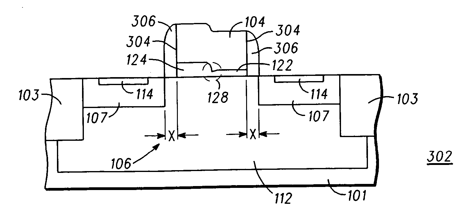
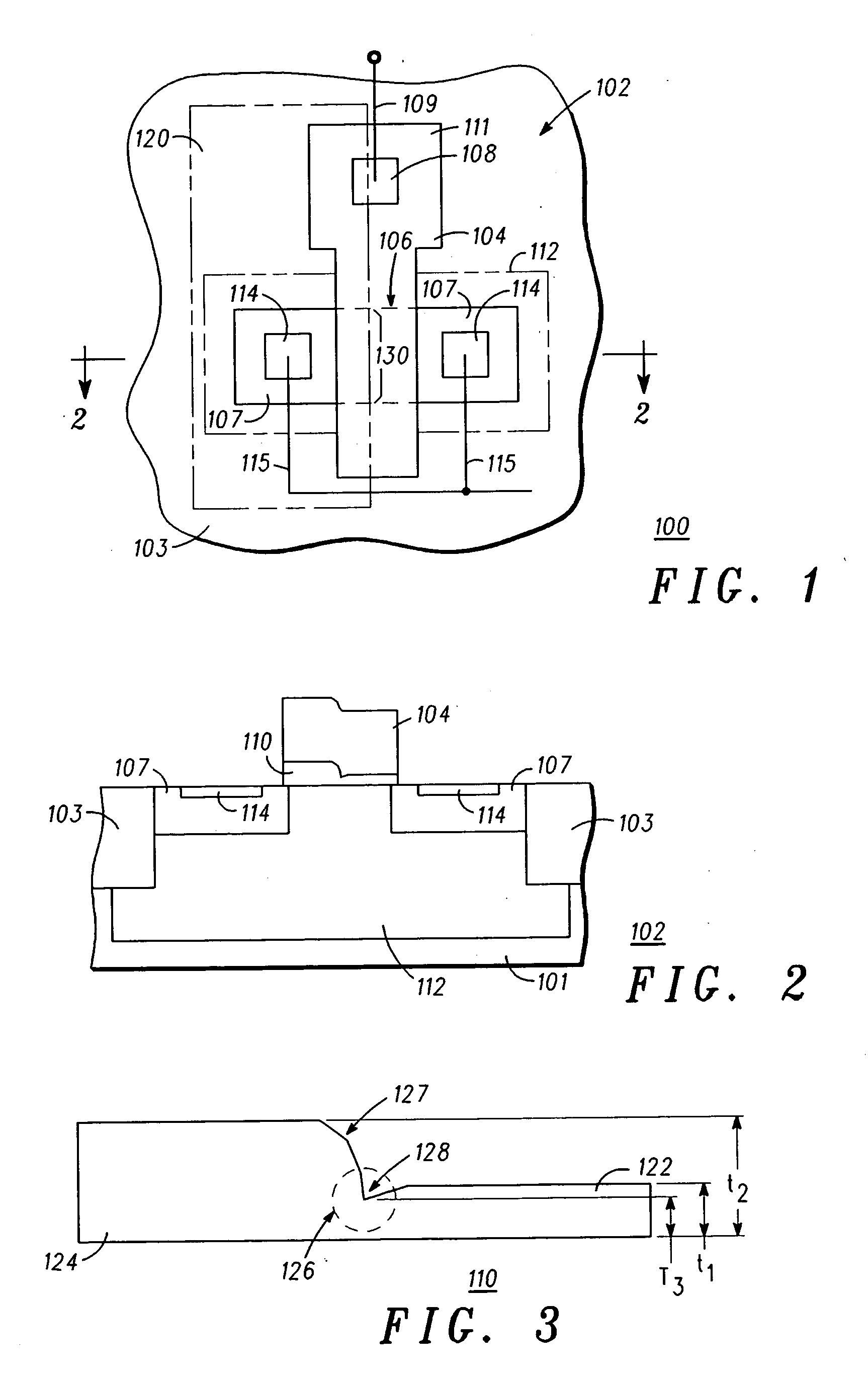
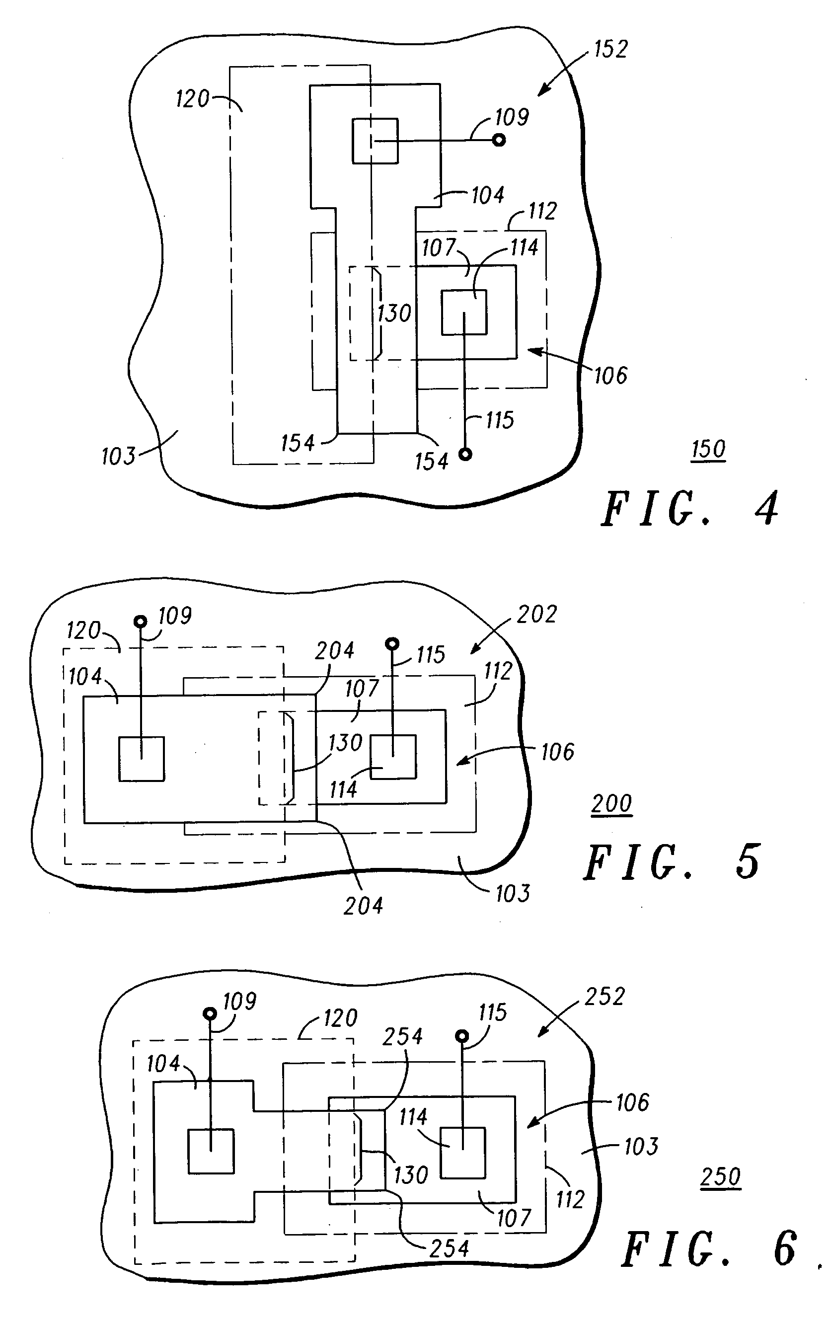
[0013] In accordance with the present invention, there is provided an antifuse element utilizing a unique gate oxide and method of forming the antifuse element. The FIGs. included herein illustrate an antifuse built on a NMOS transistor, however, it should be understood that the antifuse element of the present invention can be built on a PMOS transistor or MOS capacitor.
[0014] Turning now to the drawings, FIGS. 1-6 are top and cross sectional views of an embodiment of an antifuse element according to the present invention. A semiconductor device 100, more particularly an antifuse element 102, is formed as a unique gate capacitor comprising a gate mat...
PUM
 Abstract
Description
Claims
Application Information
 - R&D Engineer
- R&D Manager
- IP Professional
- Industry Leading Data Capabilities
- Powerful AI technology
- Patent DNA Extraction
Browse by: Latest US Patents, China's latest patents, Technical Efficacy Thesaurus, Application Domain, Technology Topic.
© 2024 PatSnap. All rights reserved.Legal|Privacy policy|Modern Slavery Act Transparency Statement|Sitemap