Semiconductor device and method of manufacturing the same
- Summary
- Abstract
- Description
- Claims
- Application Information
AI Technical Summary
Benefits of technology
Problems solved by technology
Method used
Image

Examples
first embodiment
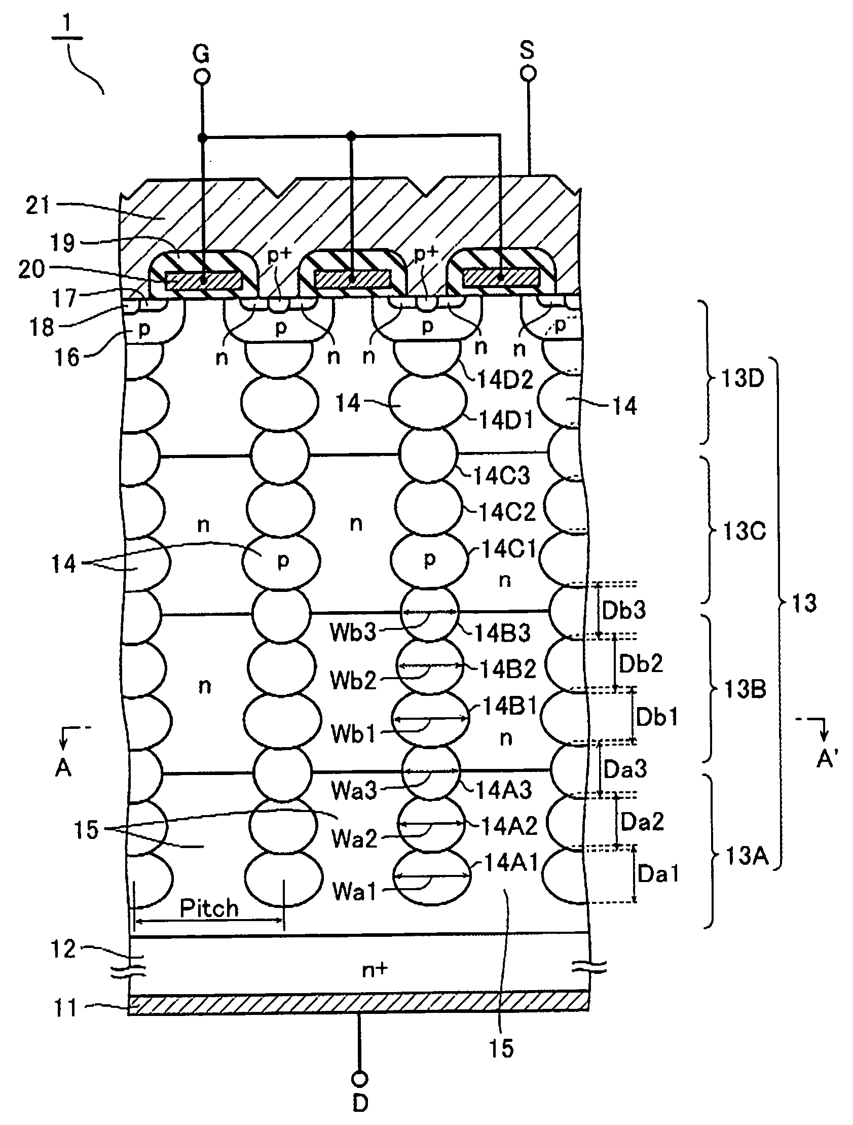
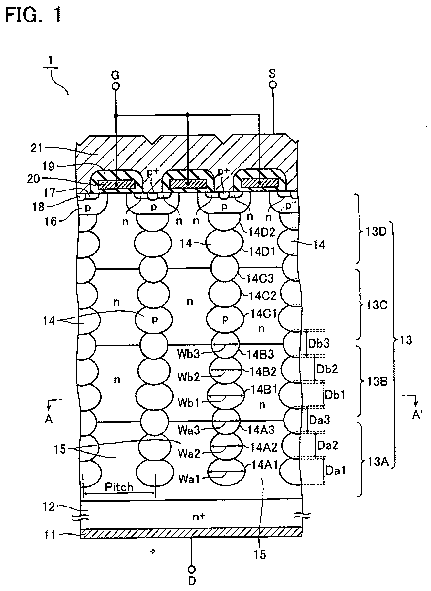
[0045]FIG. 1 is a cross-sectional view schematically illustrative of an arrangement of a power MOSFET according to a first embodiment of the present invention. The MOSFET 1 includes an n-type epitaxial layer 13 on a surface of an n+-type drain layer 12. In the n-type epitaxial layer 13, p-type pillars 14 are formed at a certain pillar pitch, Pitch. The p-type pillars 14, and n-type pillars 15 each sandwiched between the p-type pillars 14 and formed in the n-type epitaxial layer 13 form a superjunction structure. The p-type pillars 14 and the n-type pillars 15 in this embodiment are designed to have respective striped shapes extending in the direction normal to the page.
[0046] In a surface of the p-type pillar 14, a p-type base layer 16 is selectively formed by diffusion, and in a surface of the p-type base layer 16, an n-type source layer 17 and a p+-type contact layer 18 are selectively formed by diffusion. The p-type base layer 16 and the n-type source layer 17 are also designed ...
second embodiment
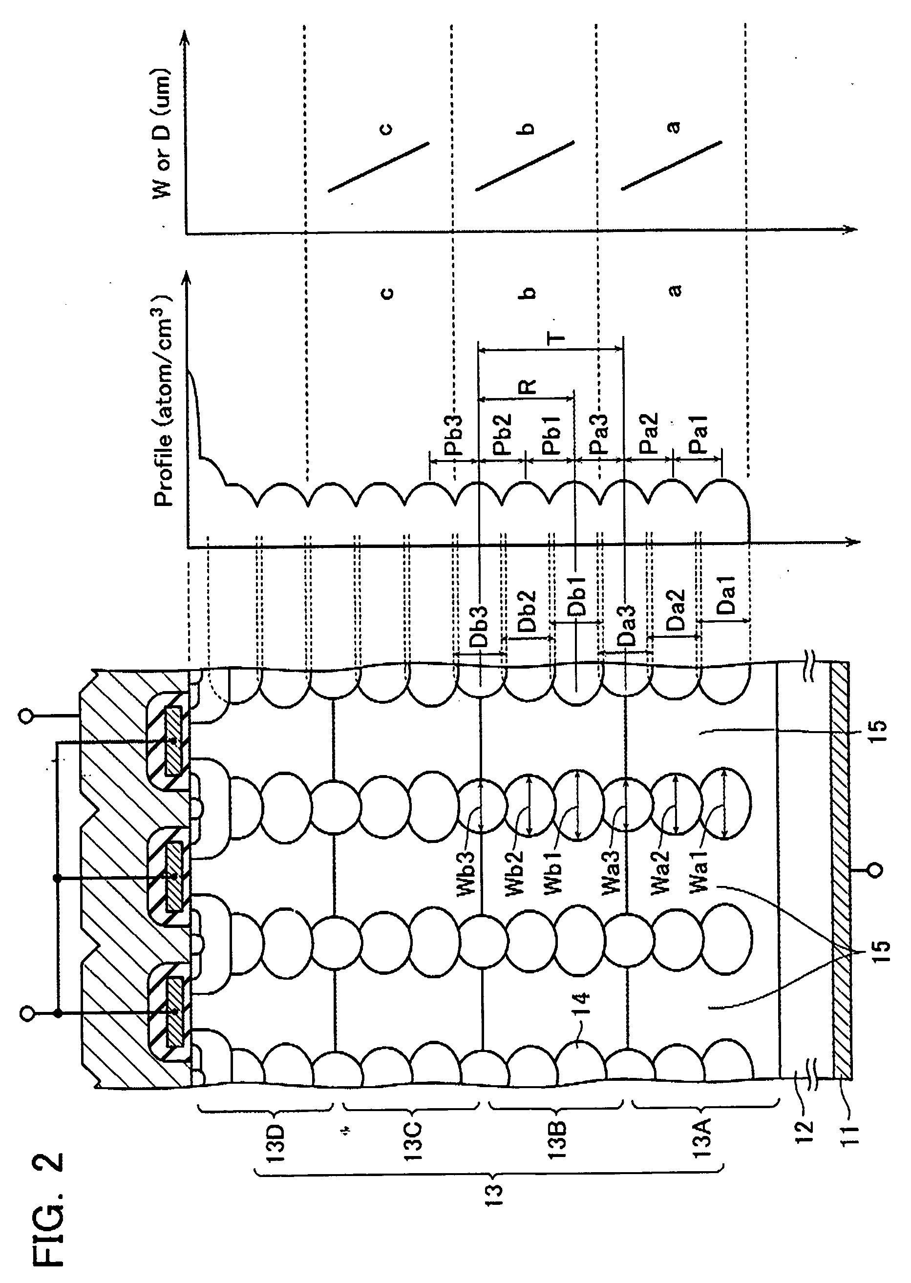
[0066]FIG. 15A shows a cross-sectional view schematically illustrative of an arrangement of a power MOSFET 1 according to a second embodiment of the present invention. FIG. 15A also shows a graph of a distribution of impurity concentrations in a p-type pillar 14, and a graph of lateral widths W and vertical depths D in a diffusion layer 14X. The components similar to those in the first embodiment are given the same reference numerals and omitted from the following detailed description. In this embodiment, the diffusion layers 14X present in the upper epitaxial layers 13C, 13D are controlled to have higher impurity concentrations. As a result, the impurity concentration in the p-type pillar 14 at the side close to the surface (the source electrode 21) is made higher than that at the side close to the bottom (the drain electrode 11).
[0067] In this embodiment, if the impurity concentrations in the epitaxial layers 13A-13D are uniform, in the upper layer portions of the pillar layer th...
third embodiment
[0073]FIG. 16 shows a cross-sectional view schematically illustrative of an arrangement of a power MOSFET 1 according to a third embodiment of the present invention. In this embodiment, not only the p-type pillar 14, but also the n-type pillar 15 is coupled along the depth, different from the preceding embodiments. Between the portions that contain ion-implanted boron therein to form the p-type pillars 14 (see FIG. 7 and so forth), an n-type impurity or phosphorous (P) is ion-implanted through a similar method to form the pillar layer as shown in FIG. 16. In this case, the impurity concentration in the n-type pillar 15 is determined in the ion implantation step. Therefore, the epitaxial layer serving as the underlying object for ion implantation can be designed to have a high resistance (low impurity concentration). In addition, the p-type pillar 14 and the n-type pillar 15 can be easily charge-balanced with each other. The achievement of the charge balance makes it possible to furt...
PUM
 Abstract
Description
Claims
Application Information
 - Generate Ideas
- Intellectual Property
- Life Sciences
- Materials
- Tech Scout
- Unparalleled Data Quality
- Higher Quality Content
- 60% Fewer Hallucinations
Browse by: Latest US Patents, China's latest patents, Technical Efficacy Thesaurus, Application Domain, Technology Topic, Popular Technical Reports.
© 2025 PatSnap. All rights reserved.Legal|Privacy policy|Modern Slavery Act Transparency Statement|Sitemap|About US| Contact US: help@patsnap.com