Semicondutor device and manufacturing method thereof

a technology of semiconductor devices and semiconductors, applied in the field of metal oxide semiconductor devices, can solve the problems of mos transistor operation, mos transistor electric field drain region is lower, and the channel dimension cannot be unlimitedly reduced, etc., to achieve the effect of reducing the electric field of the drain region and reducing the short channel

Active Publication Date: 2007-01-18
PROMOS TECH INC
View PDF3 Cites 30 Cited by
  • Summary
  • Abstract
  • Description
  • Claims
  • Application Information

AI Technical Summary

Benefits of technology

The technical effect of this patent is that it describes how to create a semiconductor device with better performance by adding a layer of material called a dielectric barrier between certain parts of the device. This helps reduce an issue known as the short-channel effect which can affect devices' ability to function properly.

Problems solved by technology

The technical problem addressed in this patent is how to suppress the short channel effect and punch through effect in MOS transistors as they are being reduced in size, while also preventing the diffusion of dopants during fabrication and hindering further size reduction and increased integration of the semiconductor device.

Method used


Image

  • Semicondutor device and manufacturing method thereof
  • Semicondutor device and manufacturing method thereof
  • Semicondutor device and manufacturing method thereof

Examples


Embodiment Construction

[0041] Reference will now be made in detail to the present preferred embodiments of the invention, examples of which are illustrated in the accompanying drawings. Wherever possible, the same reference numbers are used in the drawings and the description to refer to the same or like parts. It is to be understood that both the foregoing general description and the following detailed description are exemplary, and are intended to provide further explanation of the invention as claimed.

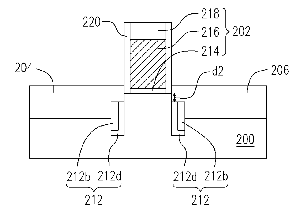
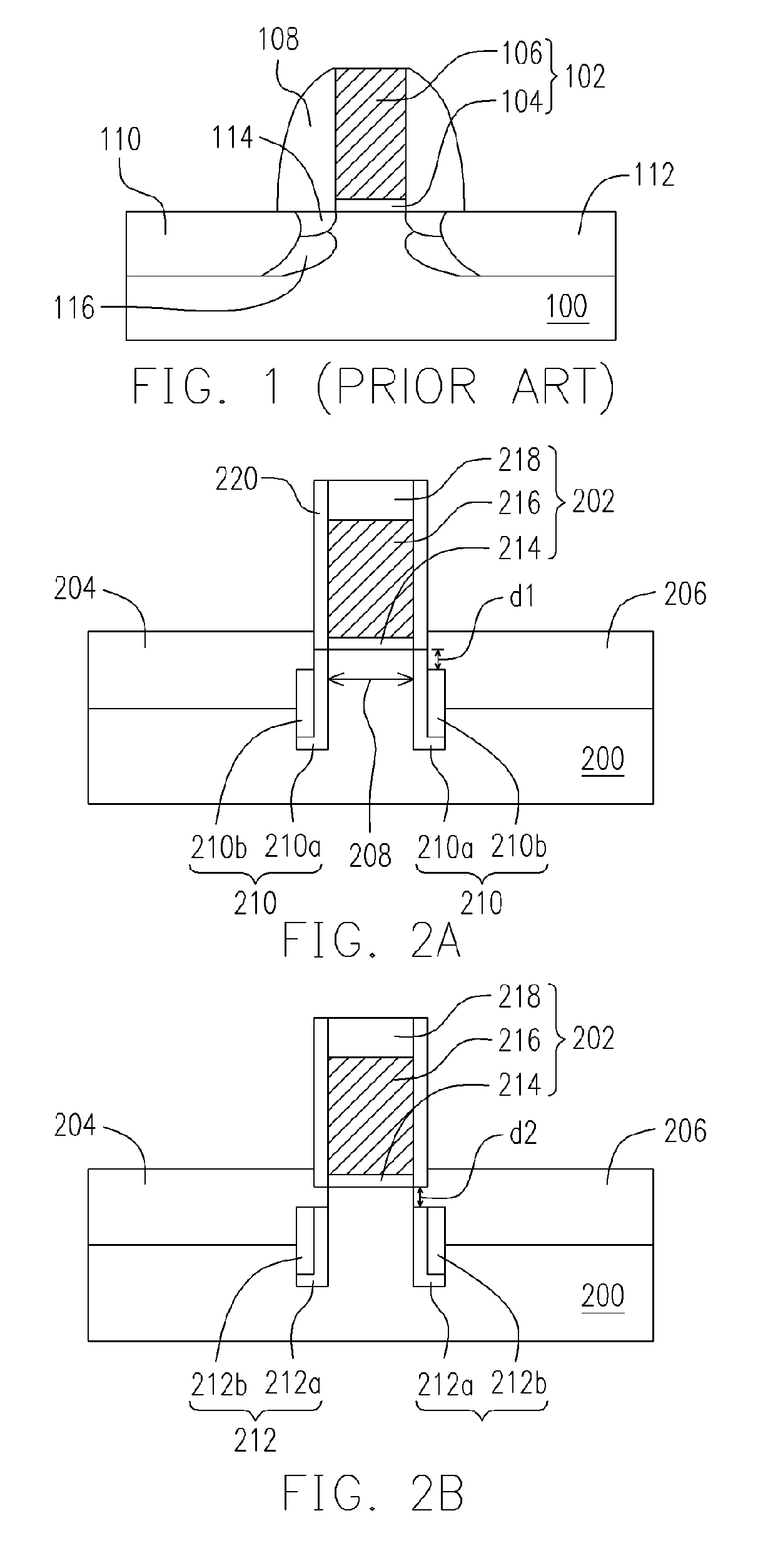
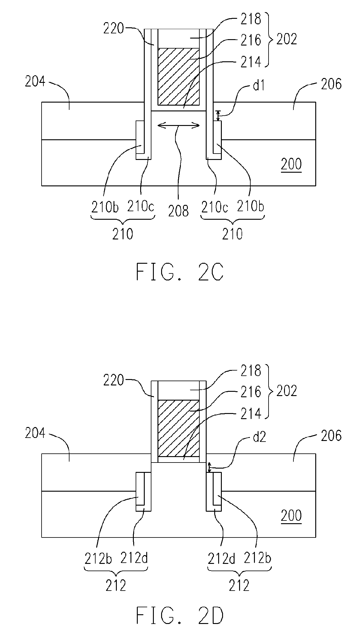
[0042]FIG. 2A is a schematic, cross-sectional diagram of a semiconductor device according to one embodiment of the present invention.

[0043] Referring to FIG. 2A, the semiconductor device of the present invention is constituted with at least a substrate 200, a gate structure 202, a source region 204, a drain region 206, and a dielectric barrier layer 210.

[0044] The gate structure 202 is disposed over a substrate 200. The gate structure 202 includes a gate dielectric layer 214, a gate conductive layer 21...


PUM


Abstract

A semiconductor device is provided. The semiconductor device has a gate structure, a source region, a drain region, and a pair of dielectric barrier layers. The gate structure is formed on a substrate. The source region and the drain region are formed in the substrate next to the gate structure, and a channel region is formed between the source region and the drain region underneath the gate structure. The pair of dielectric barrier layers is respectively formed in the substrate underneath the gate structure between the source region and the drain region. The dielectric barrier layers are used for reducing the drain induced barrier lowering effect in a nanometer scale device.

Description


Claims


Application Information

Patent Timeline
Owner PROMOS TECH INC
Why Eureka
Try Eureka