Matching circuit
a matching circuit and circuit technology, applied in the field of matching circuits, can solve the problems of difficult manufacturing, increased power consumption of the entire amplifier, and loss of circuit stability,
- Summary
- Abstract
- Description
- Claims
- Application Information
AI Technical Summary
Problems solved by technology
Method used
Image

Examples
second embodiment
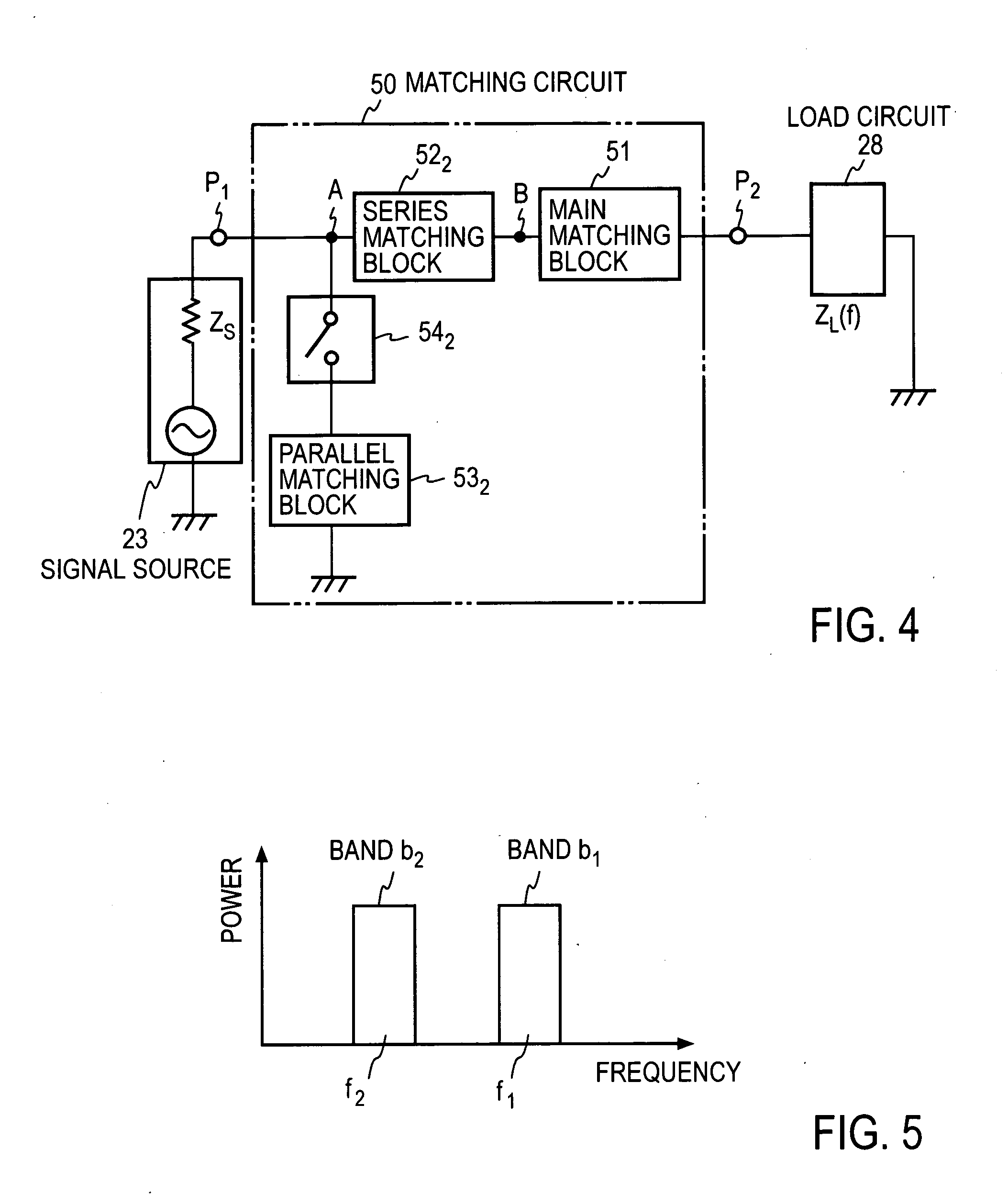
[0062]FIG. 9 shows the matching circuit 50. This embodiment assumes a case where the impedance of a signal source 23 has a frequency characteristic such as an FET does and the impedance ZL of a load circuit 28 is constant at various frequencies. This embodiment has the structure of the embodiment of the matching circuit 50 shown in FIG. 4 with the positions of the main matching block 51 and the series matching block 522 between the ports P1 and P2 switched round so that the main matching block 51 is located closer to the signal source 23 which has a frequency characteristic and with the parallel matching block 532 connected to the port P2 side through the switch 542. The principle of operation is the same as that in FIG. 4 and explanations thereof will be omitted.
third embodiment
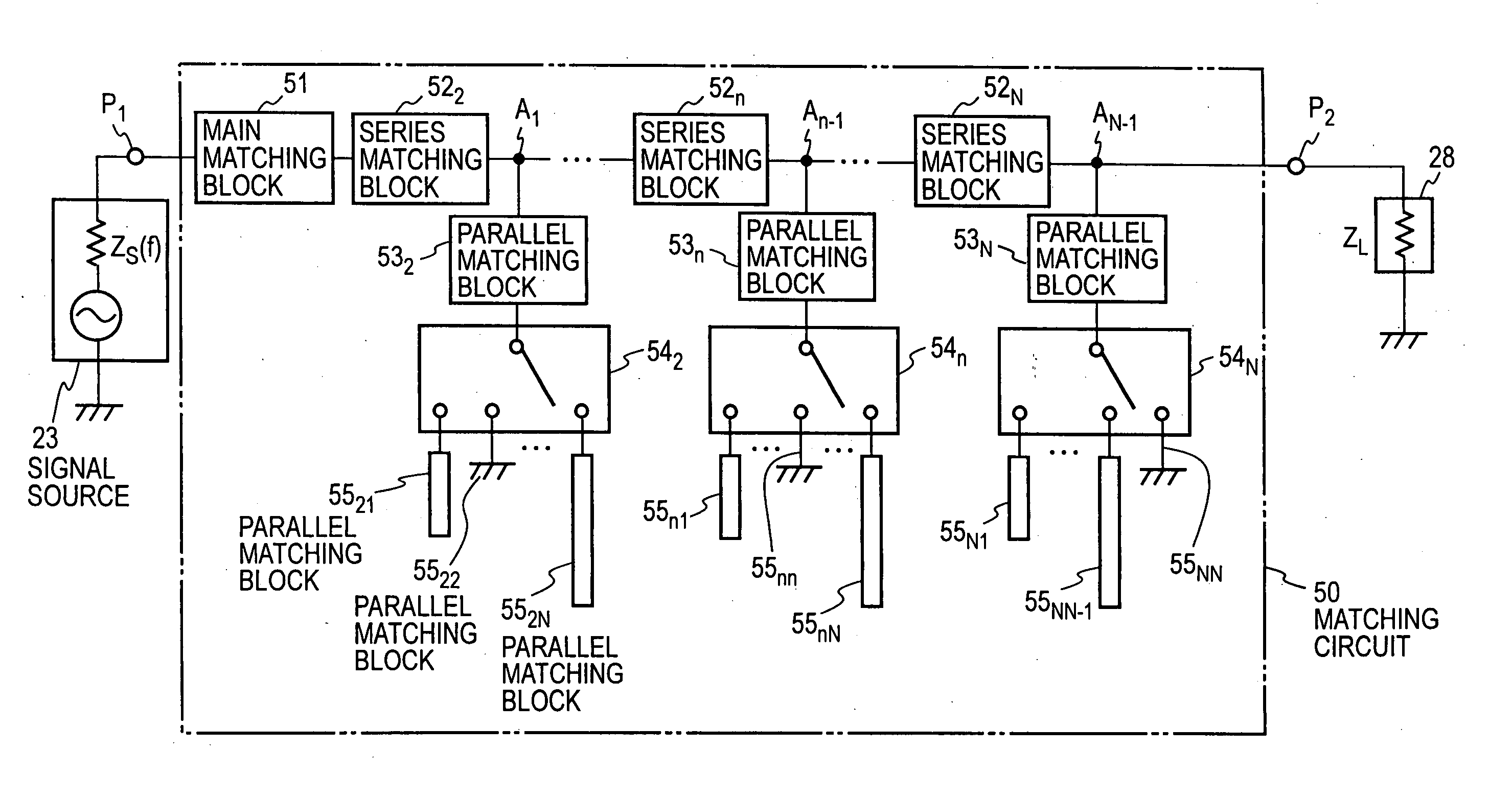
[0063]FIG. 10 shows the matching circuit 50 of the present invention. The embodiment in FIG. 10 is provided with a cascade connection of (N−1) stages (N is an integer of 3 or greater in this embodiment), each stage having a combination similar to that of a series matching block 522, a parallel matching block 532 and a switch 542 so as to operate as a matching circuit for signals of N frequency bands b1 to bN shown in FIG. 11. The embodiment in FIG. 10 corresponds to an expansion of the embodiment in FIG. 4 and by setting the nth (n: integer of 2 to N) switch 54n to ON, it is possible to change the entire matching circuit 50 to a matching circuit for an input signal of a center frequency fn with the corresponding nth parallel matching block 53n connected in parallel, series matching blocks 522 to 52N and main matching block 51.
[0064] Furthermore, by setting an arbitrary combination of (N−1) switches 542 to 54N to ON simultaneously to select parallel matching blocks connected to the s...
fourth embodiment
[0066]FIG. 13 illustrates the matching circuit of the present invention. In this embodiment, a 1-input N-output switch (single pole N throw switch) SW1 connected to a port P1 and a N-input 1-output switch (single pole N throw switch) SW2 whose output side is connected to the main matching block 51 are provided and a directly connected line 58, having a characteristic impedance Zs and (N−1) matching blocks 592 to 59N are connected to N input / output terminals between the switches SW1, SW2 in a selectable manner.
[0067] The embodiment in FIG. 13 as well as the embodiment in FIG. 10 operates as the matching circuit 50 for signals of the N frequency bands shown in FIG. 11. The main matching block 51 is a matching circuit for an input signal of a frequency f1. In order to make the entire matching circuit 50 as the matching circuit of the frequency f1, the two switches, that is, 1-input N-output switch SW1 and N-input 1-output switch SW2 are switched to the first output and the first input,...
PUM
 Abstract
Description
Claims
Application Information
 - R&D Engineer
- R&D Manager
- IP Professional
- Industry Leading Data Capabilities
- Powerful AI technology
- Patent DNA Extraction
Browse by: Latest US Patents, China's latest patents, Technical Efficacy Thesaurus, Application Domain, Technology Topic.
© 2024 PatSnap. All rights reserved.Legal|Privacy policy|Modern Slavery Act Transparency Statement|Sitemap