Light-emitting device and manufacturing method thereof

a technology of light-emitting devices and manufacturing methods, which is applied in the direction of solid-state devices, electric lighting sources, and light-emitting elements. it can solve the problems of limited area for forming light-emitting elements, point defects, and line defects, so as to improve the yield of forming light-emitting devices, the degree of freedom of each step can be increased, and the process can be flexible changed

Active Publication Date: 2007-02-08
SEMICON ENERGY LAB CO LTD
View PDF29 Cites 72 Cited by
  • Summary
  • Abstract
  • Description
  • Claims
  • Application Information

AI Technical Summary

Benefits of technology

[0023] In the invention, a light-emitting element and a driver circuit of the light-emitting element are formed over different substrates, and thus the step of forming a light-emitting element and the step of forming a driver circuit of the light-emitting element are separately performed. Therefore, degrees of freedom of each step can be increased, and the process can be flexibly changed. Although a conventional light-emitting device is manufactured by forming a planarizing film over a driver circuit of a light-emitting element first, and then forming a

Problems solved by technology

Therefore, the area for forming the light-emitting elements has been limited.
In addition, there may be a case where a coverage defect occurs due to steps resulting

Method used


Image

  • Light-emitting device and manufacturing method thereof
  • Light-emitting device and manufacturing method thereof
  • Light-emitting device and manufacturing method thereof

Examples


embodiment mode 1

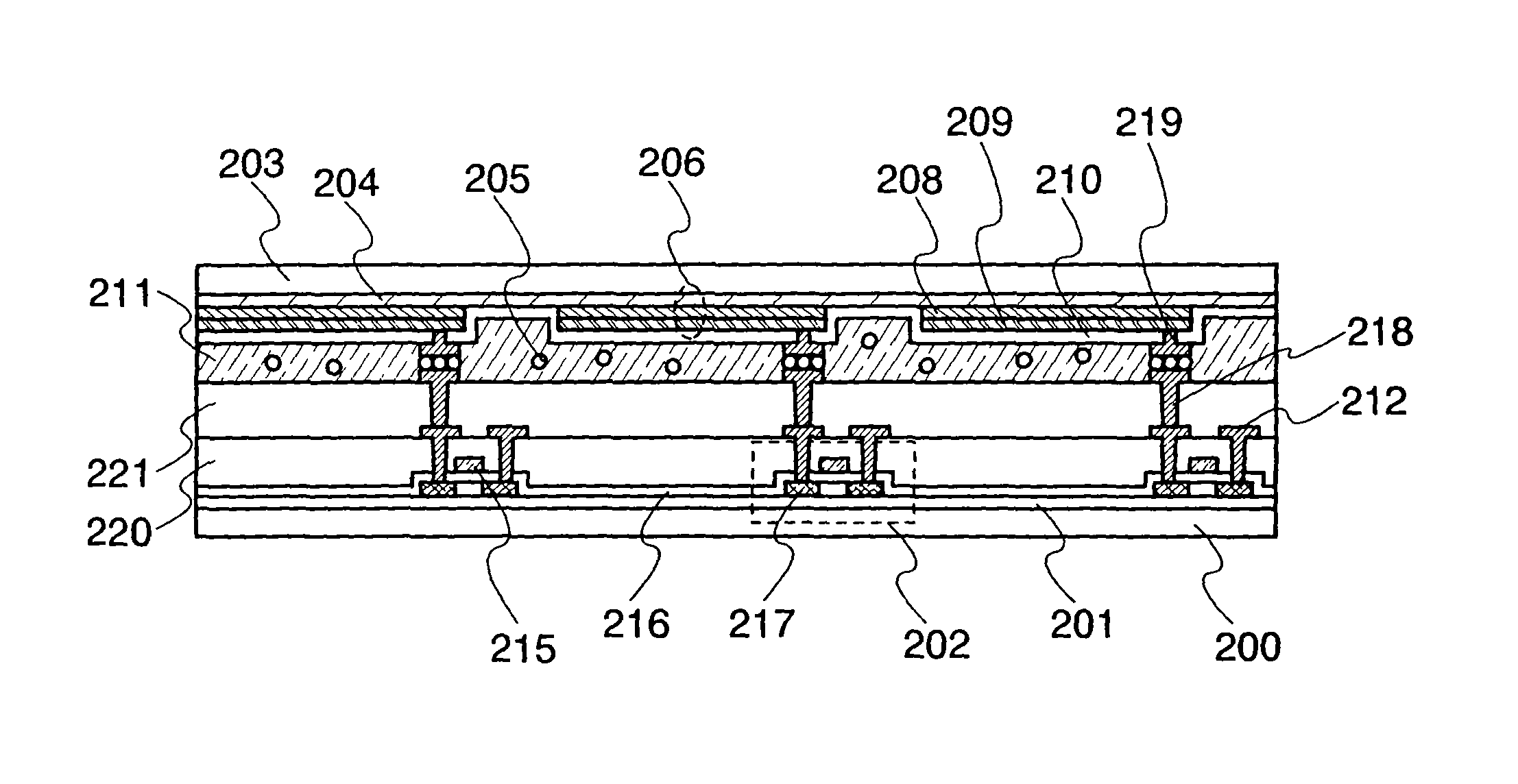
[0060] In this embodiment mode, description is made of the first example of an active matrix light-emitting device where a light-emitting element formed over a first substrate and a transistor formed over a second substrate are electrically connected. That is, description is made of the first example where the light-emitting device with the first structure of the invention is an active matrix light-emitting device.

[0061]FIG. 10 illustrates a schematic view of an active matrix light-emitting device. As shown in FIG. 10, the active matrix light-emitting device includes source signal lines (S1 to Sx), gate signal lines (G1 to Gy), a pixel portion 601, a source signal line driver circuit 602, and a gate signal line driver circuit 603.

[0062]FIG. 11 illustrates an equivalent circuit diagram of the pixel portion 601. In the pixel portion 601, a plurality of pixels 604, which are formed to be surrounded by the source signal lines (S1 to Sx), power supply lines (V1 to Vx), and the gate sig...

embodiment mode 2

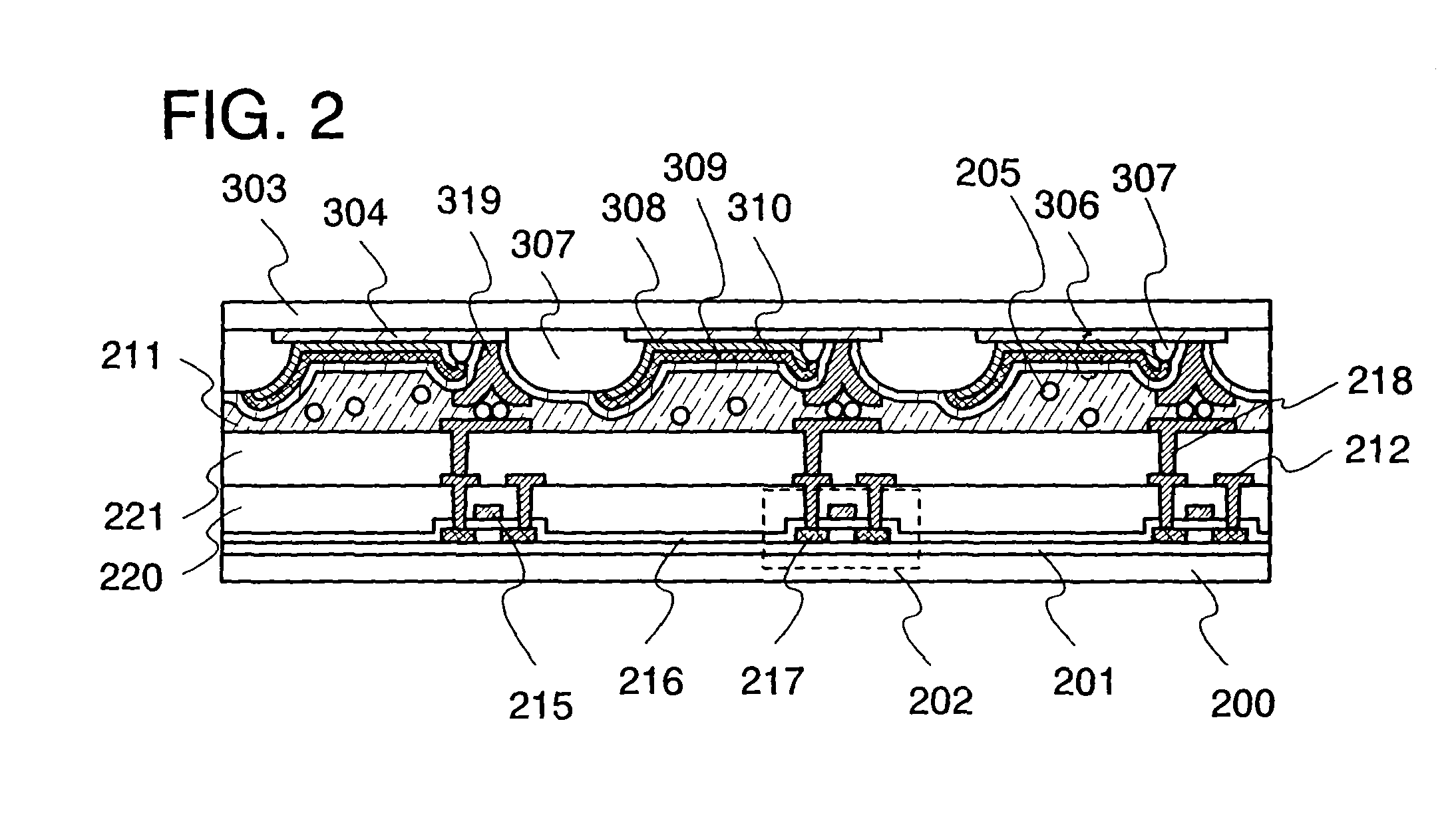
[0106] In this embodiment mode, description is made of the second example of an active matrix light-emitting device, where a light-emitting element formed over a first substrate and a transistor formed over a second substrate are electrically connected. That is, description is made of the second example of a case where the light-emitting device with the first structure of the invention is an active matrix light-emitting device.

[0107] The light-emitting device in this embodiment mode has a light-emitting element with a cross-sectional structure which differs from that shown in Embodiment Mode 1. Note that description will be made by using the pixel circuit 609 shown in FIG. 12 as an illustrative configuration of a pixel circuit as in Embodiment Mode 1.

[0108] In the light-emitting device shown in this embodiment mode, the structure of the components over the second substrate is similar to that in Embodiment Mode 1; therefore, description of the second substrate is omitted, and the s...

embodiment mode 3

[0133] In this embodiment mode, description is made of the third example of an active matrix light-emitting device, where a light-emitting element formed over a first substrate and a transistor formed over a second substrate are electrically connected. That is, description is made of the third example of a case where the light-emitting device with the first structure of the invention is an active matrix light-emitting device.

[0134] The light-emitting device in this embodiment mode has a light-emitting element with a cross-sectional structure which differs from that shown in Embodiment Modes 1 and 2. Note that description will be made by using the pixel circuit 609 shown in FIG. 12 as an illustrative configuration of a pixel circuit as in Embodiment Modes 1 and 2.

[0135] In the light-emitting device shown in this embodiment mode, the structure of the components over the second substrate is similar to that in Embodiment Mode 1; therefore, description of the second substrate is omitte...


PUM


Abstract

To prevent a point defect and a line defect in forming a light-emitting device, thereby improving the yield. A light-emitting element and a driver circuit of the light-emitting element, which are provided over different substrates, are electrically connected. That is, a light-emitting element and a driver circuit of the light-emitting element are formed over different substrates first, and then electrically connected. By providing a light-emitting element and a driver circuit of the light-emitting element over different substrates, the step of forming the light-emitting element and the step of forming the driver circuit of the light-emitting element can be performed separately. Therefore, degrees of freedom of each step can be increased, and the process can be flexibly changed. Further, steps (irregularities) on the surface for forming the light-emitting element can be reduced than in the conventional technique.

Description

BACKGROUND OF THE INVENTION [0001] 1. Field of the Invention [0002] The present invention relates to a light-emitting device and a manufacturing method thereof. [0003] 2. Description of the Related Art [0004] Conventionally, a light-emitting device having light-emitting elements has been formed through the following steps of: 1) forming a semiconductor circuit for driving light-emitting elements over a substrate such as a glass substrate by using a semiconductor process, 2) forming an insulating film (planarizing film) over the semiconductor circuit, and 3) forming light-emitting elements over the insulating film. That is, a semiconductor circuit for driving light-emitting elements and light-emitting elements are formed by stacking layers over a substrate in order from the bottom. [0005] Since a light-emitting device manufactured through the conventional manufacturing process has an insulating film over a semiconductor circuit for driving light-emitting elements, and light-emitting ...

Claims


Application Information

Patent Timeline
IPC IPC(8): H01L29/04H05B44/00
CPCH01L27/12H01L27/1214H01L27/1266H01L27/14645Y10S257/918H01L27/3253H01L27/3288H01L2227/326H01L27/3227H01L27/124H10K59/60H10K59/1275H10K59/179H10K71/80H10K59/1201
Inventor NAKAMURA, OSAMUHIGUCHI, MIYUKIWATANABE, YASUKOARAI, YASUYUKI
Owner SEMICON ENERGY LAB CO LTD
Why Eureka
Try Eureka