Clock frequency divider circuit and method of dividing clock frequency
a clock frequency and divider circuit technology, applied in the direction of pulse technique, oscillations generator, counting chain synchronous pulse counter, etc., can solve the problems of not being able to achieve the clock frequency divider circuit, the positive or negative cycle of the output clock signal is too short, and the rise edge and fall edge of the output clock signal are not ideal for the next circuit stage,
- Summary
- Abstract
- Description
- Claims
- Application Information
AI Technical Summary
Benefits of technology
Problems solved by technology
Method used
Image


Examples
second embodiment
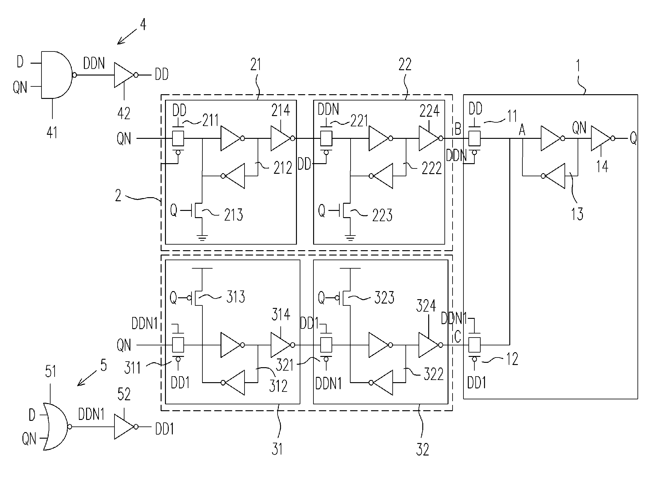
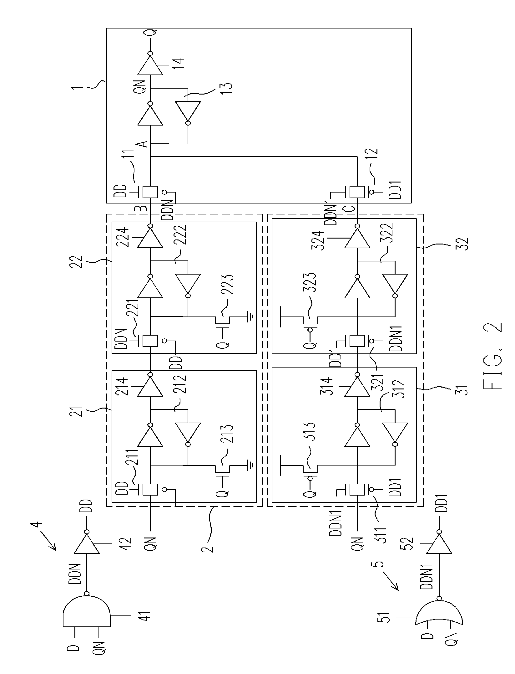
[0030] Please refer to FIGS. 4 and 5 showing a block diagram and waveforms according to the invention. As shown, the clock frequency divider circuit includes a first flip-flop circuit 1, a second flip-flop circuit 2, a third flip-flop circuit 3, a first logic control unit 4 and a second logic control unit 5. The first flip-flop circuit 1 includes two clock signal input terminals connecting to the second and third flip-flop circuits 2 and 3 respectively and two control signal input terminals connecting to the first second logic control units 4 and 5. Further, a fourth flip-flop circuit 6 is connected to the first logic control unit 4 and the second flip-flop circuit 2. The fourth flip-flop circuit 6 includes a fifth D flip-flop 61 and a sixth D flip-flop 62. If an output signal Q from the first flip-flop circuit 1 is logic 0 (which means an output signal QN is logic 1) and an external clock D is logic 0,the signal QN is input into the fifth D flip-flop 61. When the external signal D ...
third embodiment
[0031] Please refer to FIGS. 6 and 7 showing a block diagram and waveforms according to the invention. As shown, in addition to those in FIGS. 4 and 5, further, a fifth flip-flop circuit 7 is connected to the second logic control unit 5 and the third flip-flop circuit 3. The fifth flip-flop circuit 7 includes a seventh D flip-flop 71 and an eighth D flip-flop 72. If an output signal Q from the first flip-flop circuit 1 is logic 0 (which means an output signal QN is logic 1) and an external clock D is logic 0,the signal QN is input into the fifth D flip-flop 61. When the external signal D is changed into logic 1, the “logic 1” signal QN is latched in the fifth D flip-flop 61. When the external signal D is changed into logic 0,the “logic 1” signal QN is latched in the sixth D flip-flop 62. When the external signal D is changed into logic 1, the “logic 1” signal QN is latched in the first D flip-flop 21. When the external signal D is changed into logic 0,the “logic 1” signal QN is latc...
PUM
 Abstract
Description
Claims
Application Information
 - R&D
- Intellectual Property
- Life Sciences
- Materials
- Tech Scout
- Unparalleled Data Quality
- Higher Quality Content
- 60% Fewer Hallucinations
Browse by: Latest US Patents, China's latest patents, Technical Efficacy Thesaurus, Application Domain, Technology Topic, Popular Technical Reports.
© 2025 PatSnap. All rights reserved.Legal|Privacy policy|Modern Slavery Act Transparency Statement|Sitemap|About US| Contact US: help@patsnap.com