Rigid-flexible printed circuit board for package on package and manufacturing method

a printed circuit board and rigid-flexible technology, applied in the direction of printed circuit manufacturing, printed circuit aspects, semiconductor/solid-state device details, etc., can solve the problems of function errors, semiconductor chips can be easily damaged, and the semiconductor chip itself cannot transfer or receive an electrical signal with electricity supplied from outside, so as to reduce the thickness of the whole package and reduce the warpage of the board

Inactive Publication Date: 2007-03-15
SAMSUNG ELECTRO MECHANICS CO LTD
View PDF5 Cites 42 Cited by
  • Summary
  • Abstract
  • Description
  • Claims
  • Application Information

AI Technical Summary

Benefits of technology

[0020] Also, the present invention aims to provide a rigid-flexible printed circuit board which can lower a thickness of whole packages when same numbers of the semiconductor chips are mounted.
[0021] Also, the present invention aims to provide a rigid-flexible printed circ...

Problems solved by technology

Even though from several tens to several hundreds of chips printed with identical circuits can be placed on one wafer, semiconductor chip itself cannot transfer or receive an electrical signal with electricity supplied from outside.
Moreover, the sem...

Method used


Image

  • Rigid-flexible printed circuit board for package on package and manufacturing method
  • Rigid-flexible printed circuit board for package on package and manufacturing method
  • Rigid-flexible printed circuit board for package on package and manufacturing method

Examples


Embodiment Construction

[0043] Hereinafter, embodiments of the invention will be described in more detail with reference to the accompanying drawings. In the description with reference to the accompanying drawings, those components are rendered the same reference number that are the same or are in correspondence regardless of the figure number, and redundant explanations are omitted.

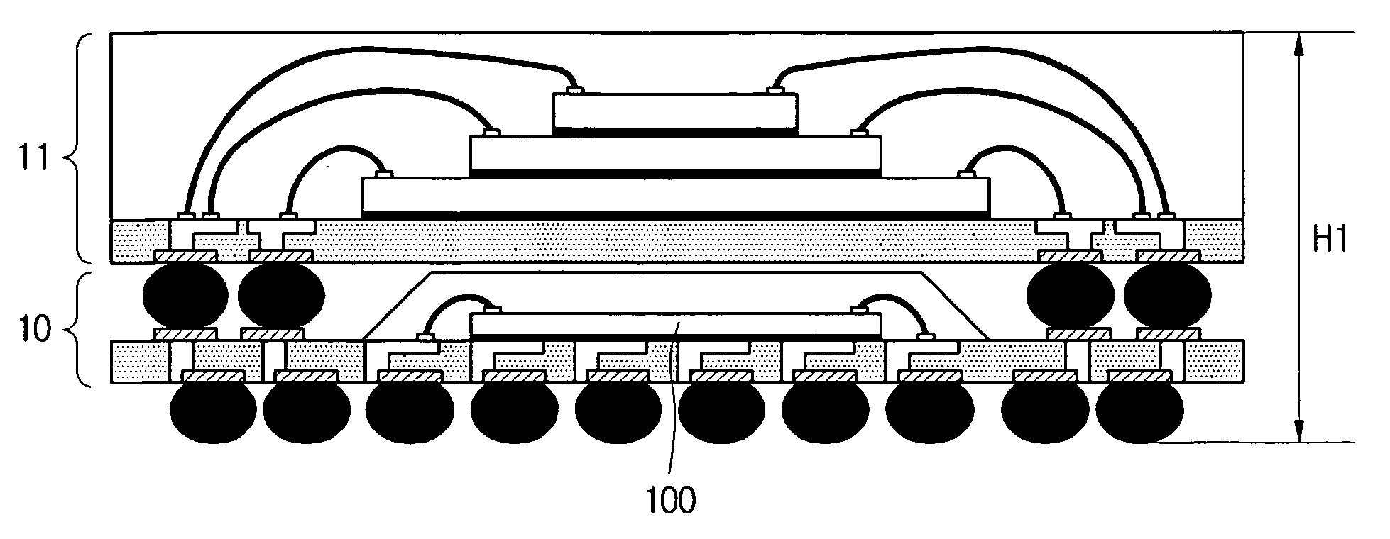
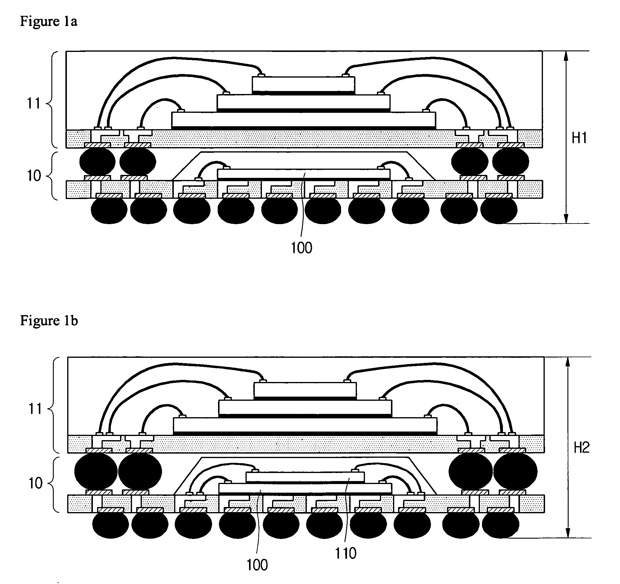
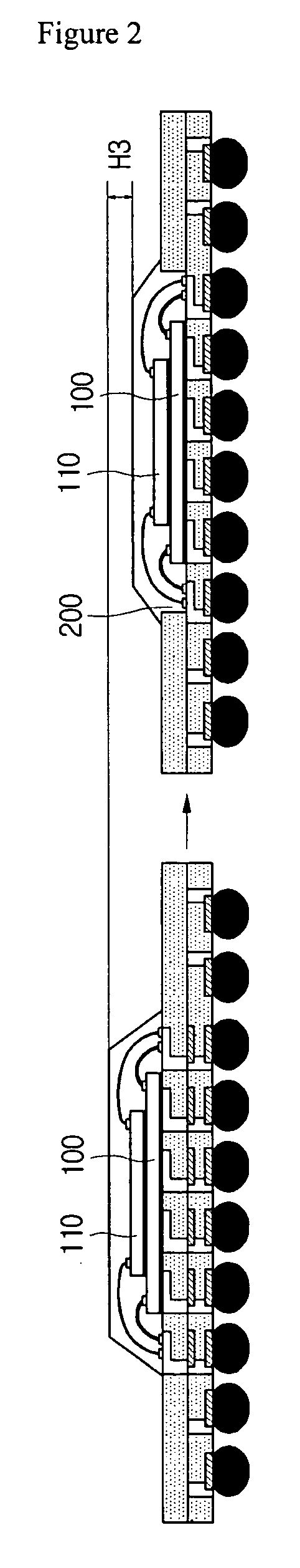
[0044]FIG. 2 shows a thinner package according to an embodiment of the present invention, in comparison with the conventional invention. A bottom substrate of a POP package is shown in FIG. 2.

[0045] Referring to FIG. 2, a package on the left side is a stack package on which 2 or more semiconductor chips 100 and 110 are mounted according to a conventional technology. A package on the right side has a cavity 200 according to an embodiment of the present invention and the semiconductor chips 100 and 110 are mounted therein so that a whole thickness of the POP package is reduced to H3. Therefore, the whole thickness of a POP pack...


PUM

PropertyMeasurementUnit
Thicknessaaaaaaaaaa
Pressureaaaaaaaaaa
Flexibilityaaaaaaaaaa

Abstract

The present invention relates to a rigid-flexible multi-layer printed circuit board comprising: a flexible substrate of which circuits are formed on both sides and which is bendable; a rigid substrate which is laminated on the flexible substrate and circuits are formed on both sides and a cavity within which a semiconductor chip is mounted is formed; and a bonding sheet adhering the flexible substrate and the rigid substrate and having a insulating property. According the present invention, when the same numbers of the semiconductor chips are mounted or the POP is embodied, the whole thickness of the package can be lower. Also, two more semiconductor chips can be mounted using the space as the thickness of the core layer, and the structure impossible when the number of semiconductor chip mounted on the bottom substrate becomes two from one in conventional technology can be embodied.

Description

CROSS-REFERENCE TO RELATED APPLICATIONS [0001] This application claims the benefit of Korean Patent Application No. 2005-0085644 filed with the Korea Industrial Property Office on Sep. 14, 2005, the disclosure of which is incorporated herein by reference in its entirety. BACKGROUND [0002] 1. Technical Field [0003] The present invention relates to a printed circuit board, in particular, to a printed circuit board for package on package and a manufacturing method thereof in which there is a level difference in the surface of the substrate for mounting 2 or more IC chips on the bottom substrate of the printed circuit board. [0004] 2. Description of the Related Art [0005] Semiconductor packaging provides electrical connection to semiconductor chips including circuits and is seal-packaged to protect from any external impact so that it allows effect on the physical function and appearance for useful in the real life. [0006] The semiconductor package is an outcome of the semiconductor pack...

Claims


Application Information

Patent Timeline
IPC IPC(8): H01L21/4763
CPCH05K1/183Y10T29/49124H05K3/4623H05K3/4691H05K2201/055H05K2201/09536H05K2201/10515H05K2203/049H05K2203/063H01L25/105H01L2224/32145H01L2224/32225H01L2224/48091H01L2224/48227H01L2224/73265H01L2924/15311H01L2924/15331H05K1/189H01L2924/00012H01L2924/00014H01L2924/00H01L24/73H01L2924/14H05K2201/056H01L2924/181H01L23/12H05K3/46
Inventor JUNG, HOE-KUKANG, MYUNG-SAMPARK, JUNG-HYUN
Owner SAMSUNG ELECTRO MECHANICS CO LTD
Why Eureka
Try Eureka