Package structure and manufacturing method thereof

a manufacturing method and technology of a package, applied in the field of multi-chip packages, can solve the problems of reducing unsuitable for portable electronic devices whose internal space is limited, and achieving the effect of increasing the space utilization of the circuit board, increasing the requirement for function, and limited internal spa

Inactive Publication Date: 2009-03-26
ADVANCED SEMICON ENG INC
View PDF3 Cites 1 Cited by
  • Summary
  • Abstract
  • Description
  • Claims
  • Application Information

AI Technical Summary

Benefits of technology

[0009]The invention is directed to a quad-flat non-leaded (QFN) multichip package capable of largely increasing the space utilization of circuit board and is applicable to a portable electronic device whose internal space is limited and requirement for function is high.

Problems solved by technology

However, it is very difficult to fabricate a lead frame in such particular shape by method of etching or punching.
However, such QFN package can only be bonded to a circuit board by itself and cannot be stacked with one another, hence decreasing the space utilization of the circuit board and being unsuitable for a portable electronic device whose internal space is limited and requirement for function is high.
However, the stackable QFN semiconductor package is disadvantaged by using a complicated substrate, not only being difficult to process but also incurring higher cost and increasing the thickness of the whole package structure.

Method used


Image

  • Package structure and manufacturing method thereof
  • Package structure and manufacturing method thereof
  • Package structure and manufacturing method thereof

Examples


Embodiment Construction

[0022]The objects, features and advantages of the invention are disclosed below in preferred embodiments of the invention with accompanying drawings.

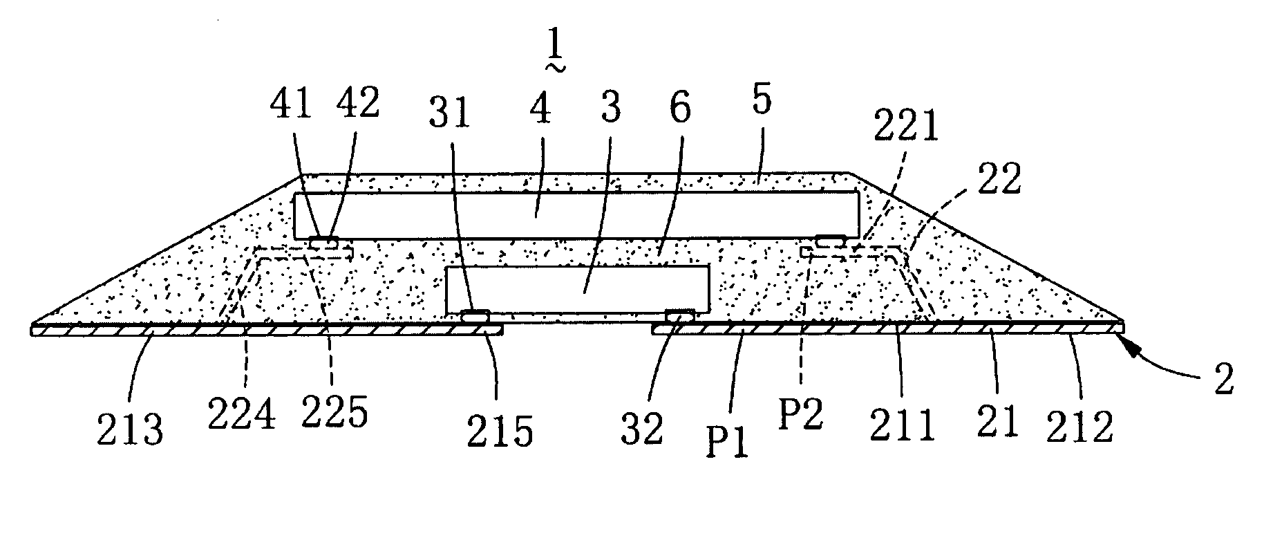
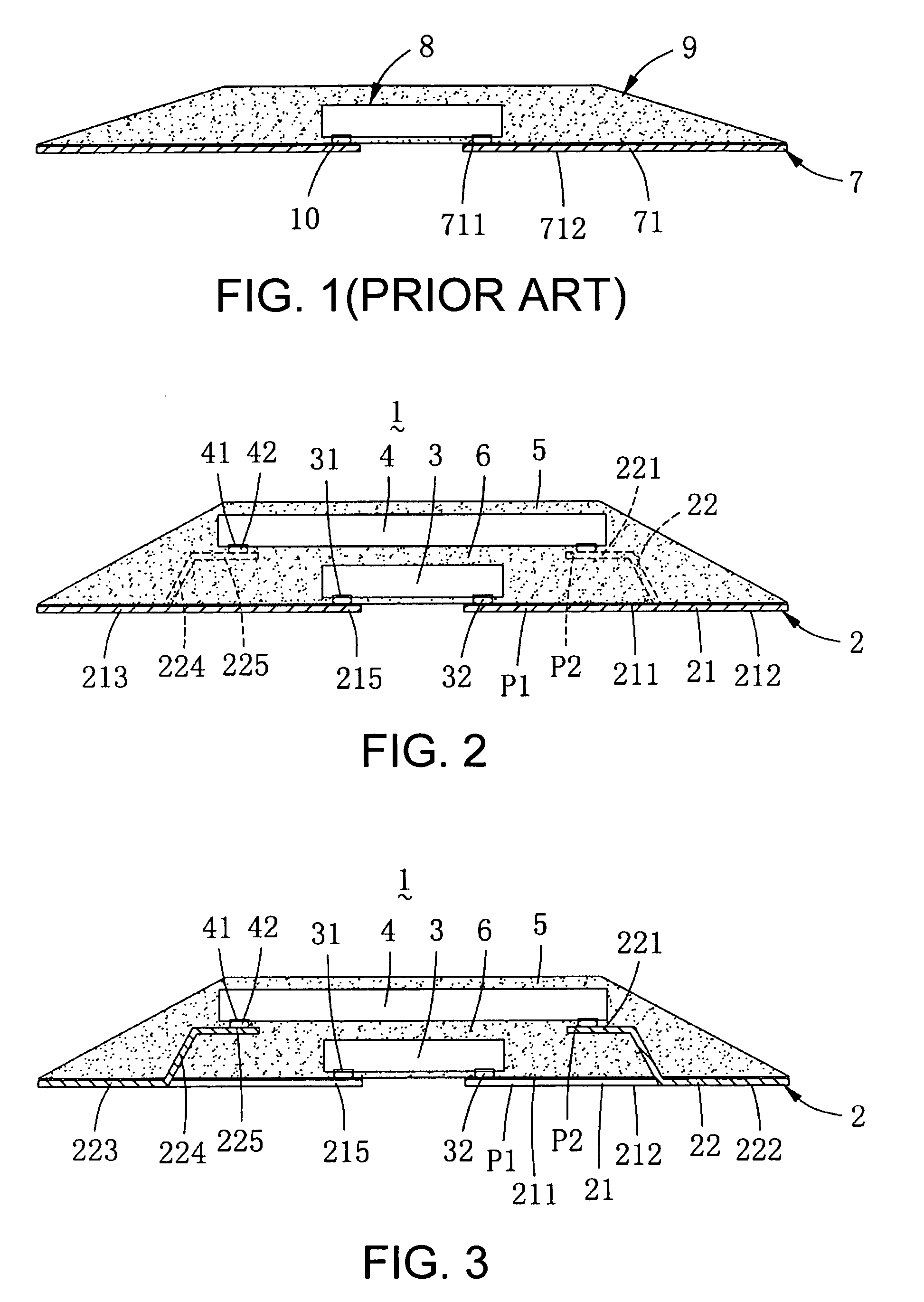
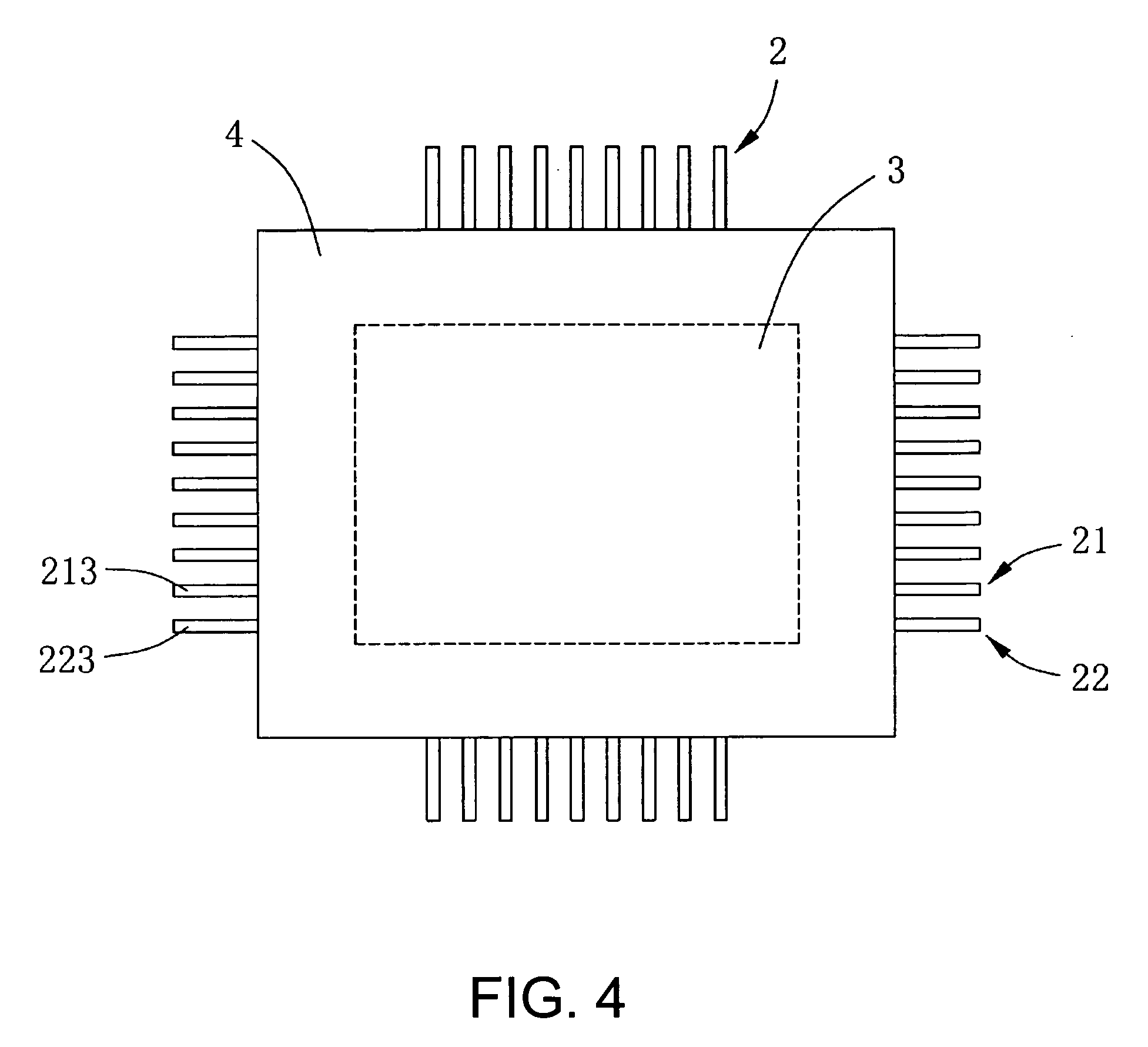
[0023]A quad-flat non-leaded (QFN) multichip package is disclosed in the invention. Referring to FIGS. 2, 3 and 4. FIG. 2 shows a cross-sectional view of a QFN multichip package according to a preferred embodiment of the invention. FIG. 3 shows another cross-sectional view of the QFN multichip package of the invention. FIG. 4 shows an upper view of a stacked structure of a chip and a lead frame of the multichip package of the invention. As indicated in FIG. 2 and FIG. 3, the QFN multichip package 1 of the invention mainly includes a lead frame 2, a first chip 3, a second chip 4 and a molding compound 5.

[0024]The lead frame 2 has a plurality of first leads 21 and second leads 22 extended to different planes, wherein each first lead 21 has a first upper surface 211 and a first lower surface 212, and each second lead 22 has a second upper ...


PUM


Abstract

A quad-flat non-leaded (QFN) multichip package and a multichip package are provided. The QFN multichip package includes a lead frame, a first chip, a second chip and a molding compound. The lead frame has a plurality of first leads and second leads alternately arranged with each other. Each first lead includes a first connection portion and a first contact portion. Each second lead includes a second connection portion, a bending part and a second contact portion. The bending part is bent upward such that an interval is formed between the second contact portion and the first contact portion. The first chip is disposed between the first leads and the second leads. The second chip is disposed above the first chip. The molding compound encloses the first chip, the second chip, the first leads and the second leads, and further exposes the lower surfaces of the first and the second leads.

Description

[0001]This application claims the benefit of Taiwan application Serial No. 96135510, filed Sep. 21, 2007, the subject matter of which is incorporated herein by reference.BACKGROUND OF THE INVENTION[0002]1. Field of the Invention[0003]The invention relates in general to a multichip package, and more particularly to a quad-flat non-leaded (QFN) multichip package.[0004]2. Description of the Related Art[0005]A generally known stackable semiconductor package is disclosed in U.S. Pat. No. 6,075,284. The inner leads of the lead frame are respectively extended upward and downward to form a pair of bumps such that the stackable package can be stacked face to face or back to back. However, it is very difficult to fabricate a lead frame in such particular shape by method of etching or punching. Moreover, that the leads of the lead frame are located at two lateral sides of the package is categorized as dual-in-line package (DIP) and cannot be used to pack die(s) with more electrodes as a quad f...

Claims


Application Information

Patent Timeline
Patent Type & Authority Applications(United States)
IPC IPC(8): H01L23/495
CPCH01L23/49551H01L23/49575H01L2224/16245H01L2924/01079H01L2224/16H01L2224/05571H01L2224/05573H01L2924/00014H01L2224/05599
Inventor PAO, CHIH-MIN
Owner ADVANCED SEMICON ENG INC
Why Eureka
Try Eureka