
Magneto-resistance transistor and method thereof

a magneto-resistance transistor and transistor technology, applied in the field of magneto-resistance transistors, can solve the problems of limiting the utilization of conventional spin transistors in lower current applications, and affecting the miniaturization efficiency of conventional spin transistors

Inactive Publication Date: 2007-03-22
IND TECH RES INST
View PDF12 Cites 0 Cited by
  • Summary
  • Abstract
  • Description
  • Claims
  • Application Information

AI Technical Summary

Problems solved by technology

However, the electric current output of conventional spin transistors may be small, thereby limiting their utilization in lower current applications (e.g., in a range from 1.287 pA to 44 pA).
Further, conventional spin transistors may be more difficult to miniaturize.
However, the GaAs substrate may have a higher cost and / or the aluminum oxide layer may not be formed as a uniform layer.
Accordingly, since only a lower electric current input may be used with the above-described conventional spin transistor, the electric current output of the conventional spin transistor may also be lower, thereby limiting their use to lower current applications.
The GaAs substrate may be expensive.
Further, the aluminum oxide layer may not be formed as a uniform layer.
Since the magneto-resistant device with a higher current fluctuation rate may require a higher-quality (i.e. uniform) layer, the complexity of the manufacturing process may increase as a more uniform aluminum oxide layer may be difficult to produce.

Method used


Image

  • Magneto-resistance transistor and method thereof
  • Magneto-resistance transistor and method thereof
  • Magneto-resistance transistor and method thereof

Examples


Embodiment Construction

[0030] Hereinafter, example embodiments of the present invention will be described in detail with reference to the accompanying drawings.

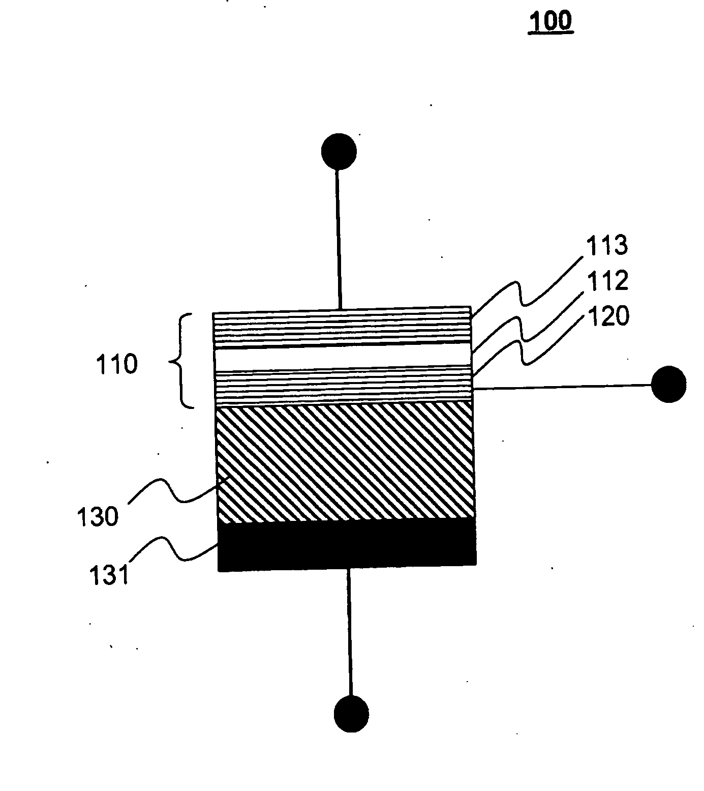
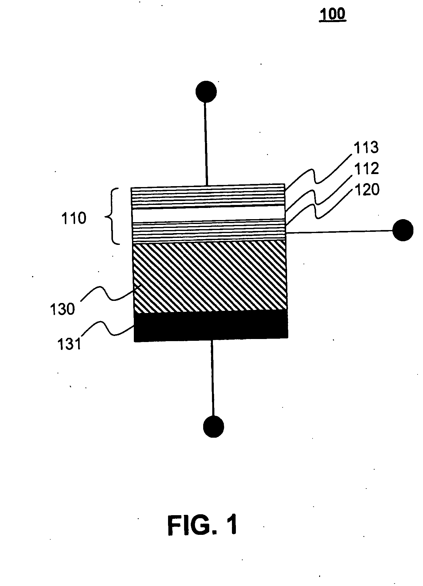
[0031]FIG. 1 illustrates a schematic view of a magneto-resistance transistor 100 according to an example embodiment of the present invention.

[0032] In another example embodiment of the present invention, referring to FIG. 1, the magneto-resistance transistor 100 may include a magneto-resistant element 110, a passive element 130 and / or an ohmic contact layer 131. As shown in FIG. 1, the magneto-resistant element. 110, the passive element 130 and / or the ohmic contact layer 131 may be stacked. Further, the magneto-resistant element 110, the passive element 130, and / or the ohmic contact layer 131 may be formed on a plane of the magneto-resistance transistor 100.

[0033] In another example embodiment of the present invention, the magneto-resistant element 110 may be an emitter.

[0034] In another example embodiment of the present invention, the passive ...


PUM


Abstract

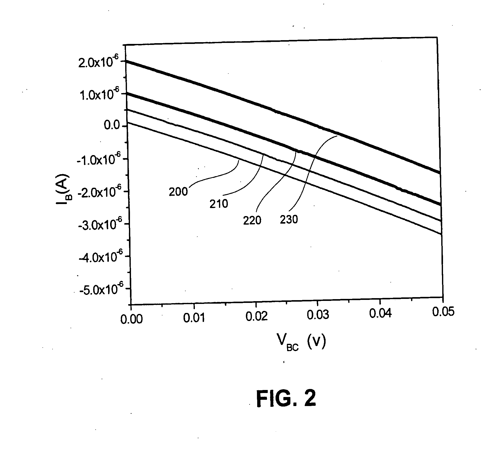
A magneto-resistance transistor including a magneto-resistant element which may function as an emitter and a passive element which may function as a collector. The base may be interposed between the passive element and the magneto-resistant element, thereby coupling the passive element with the magneto-resistant element. A magnetic field of a given strength may be applied to at least a portion of the magneto-resistant transistor, the given strength determining a resistance in the at least a portion of the magneto-resistant transistor. Thus, by adjusting the given strength of the magnetic field, the resistance may be adjusted. Therefore, different emitter current inputs may be achieved with a fixed voltage. Further, a base current may vary with a controlled variation of the emitter current input.

Description

BACKGROUND OF THE INVENTION [0001] 1. Field of Invention [0002] The present invention relates to a transistor, and more particularly to a magneto-resistance transistor and method thereof. [0003] 2. Related Art [0004] Conventional spin transistors may be electronic devices that may use a magnetic field to control an electric current. The effect of spin transistors may be similar to the effect of conventional transistors. An electron may have two spin states: spin up and spin down. The spin states of the electron may be control parameters in conventional transistors. [0005] Conventional spin transistors may have an additional control parameter, namely, a magnetic field. The magnetic field used by a conventional spin transistor may control the electric current by manipulating the spin states of electrons. Thus, electronic devices including conventional spin transistors may have enhanced functionality as compared to electronic devices including only conventional transistors. [0006] Conv...

Claims


Application Information

Patent Timeline
Patent Type & Authority Applications(United States)
IPC IPC(8): H01L43/00H01L29/82H01L27/082
CPCH01L43/08H01L29/82G11C11/161H10N50/10G11C11/15G11C11/16
Inventor HUANG, YING-WENLO, CHI-KUENYAO, YEONG-DERHSIEH, LAN-CHINJU, JAU-JIUHUANG, DER-RAY
Owner IND TECH RES INST
Learn More