Light emitting apparatus

Active Publication Date: 2007-04-05
TDK CORPARATION
View PDF5 Cites 82 Cited by
  • Summary
  • Abstract
  • Description
  • Claims
  • Application Information

AI Technical Summary

Benefits of technology

[0031] In light of the above fact, preferably, the second reflecting layer is formed on one outer surface extending in the direction parallel to the opposing direction of the plurality of internal electrodes out of the outer surfaces of the varistor element body, and the first reflecting layer is formed on the second reflecting layer so as to cover the second reflecting layer. In this case, heat generated in the semiconductor light emitting element can be efficiently transmitted to the varistor element body to be dissipated. As a result, it is feasible to suppress degradation of characteristics of the semiconductor light emitting element.
[0032] Preferably, the second reflecting layer consists of a plurality of metal layers electrically insolated from each other, and the p

Problems solved by technology

For this reason, it is difficult to achieve downsizing of the whole light emitting apparatus.
How

Method used


Image

  • Light emitting apparatus
  • Light emitting apparatus
  • Light emitting apparatus

Examples


first embodiment

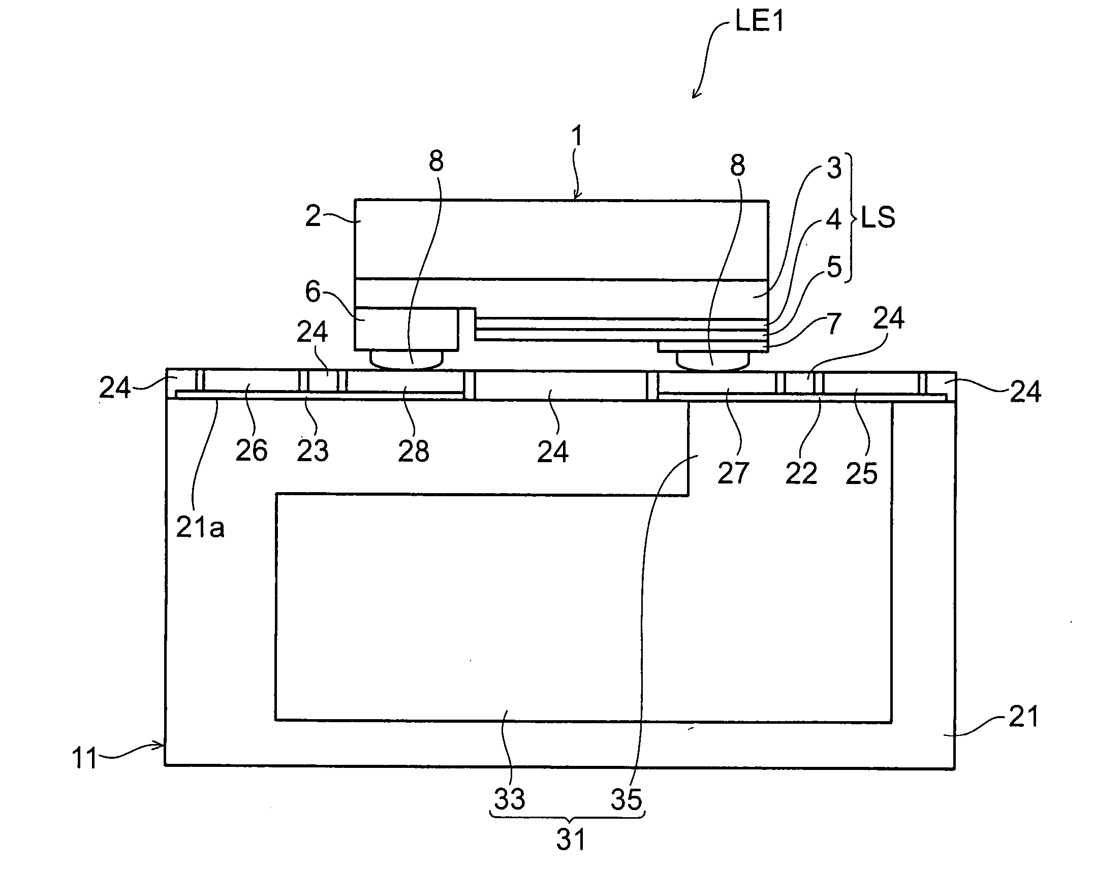
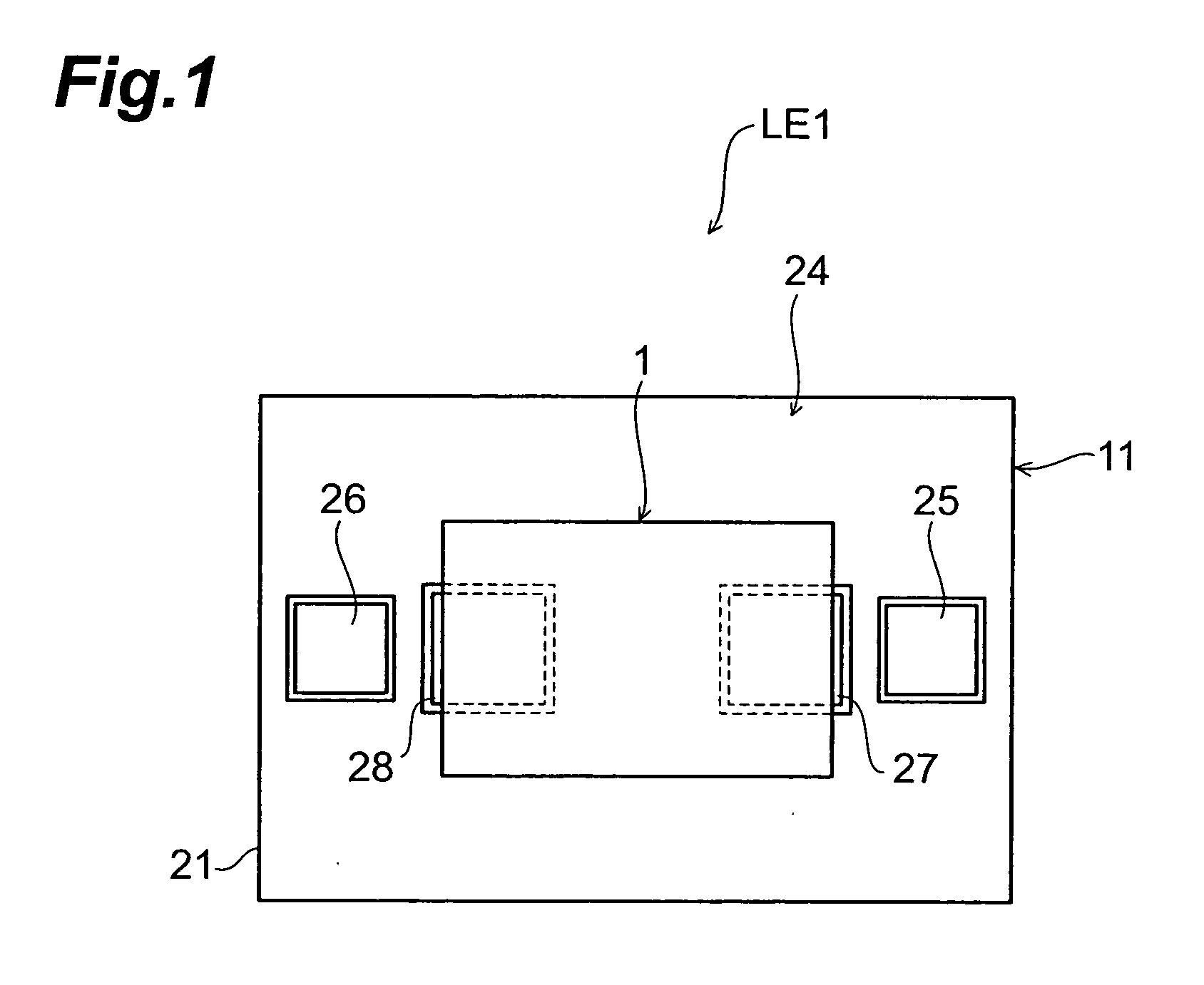
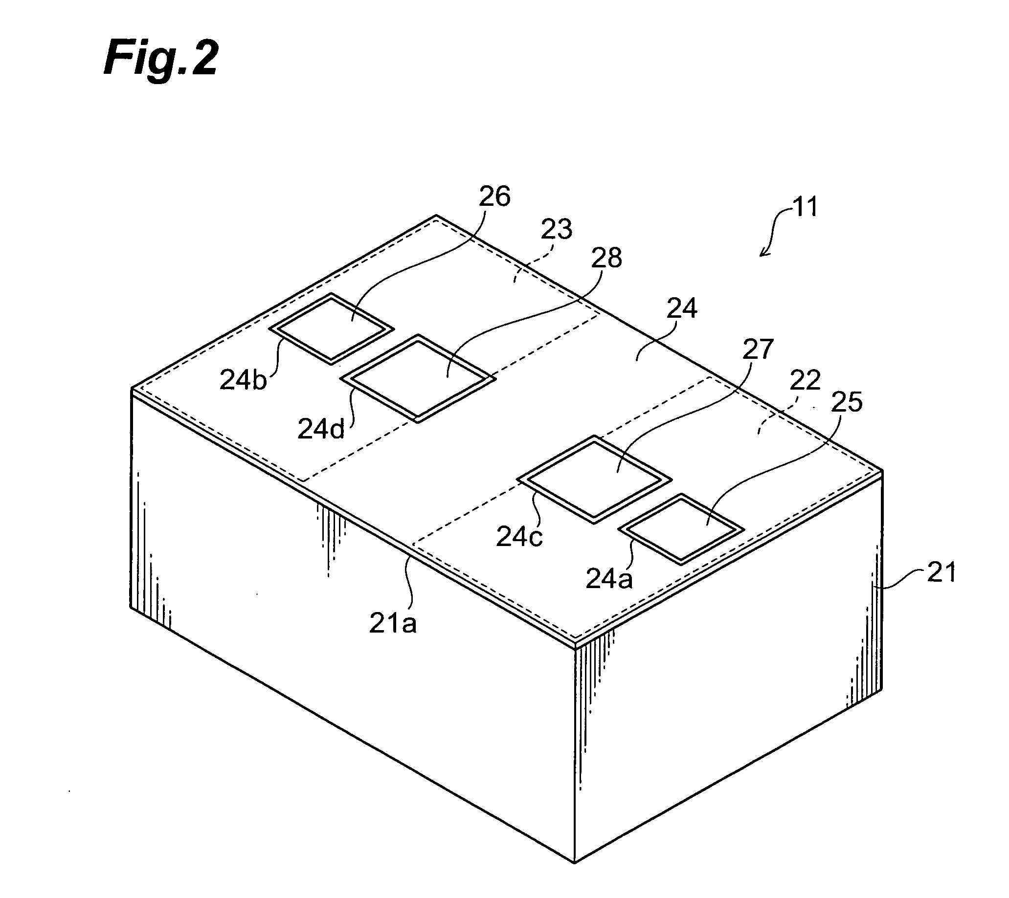
[0055] A configuration of a light emitting apparatus LE1 according to the first embodiment will be described with reference to FIGS. 1 to 5. FIG. 1 is a schematic top view showing the light emitting apparatus according to the first embodiment. FIG. 2 is a schematic perspective view showing a multilayer chip varistor in the light emitting apparatus according to the first embodiment. FIG. 3 is a schematic top view showing the multilayer chip varistor in the light emitting apparatus according to the first embodiment. FIG. 4 is a drawing for explaining a sectional configuration along line IV-IV in FIG. 3. FIG. 5 is a drawing for explaining a sectional configuration along line V-V in FIG. 3.

[0056] The light emitting apparatus LE1, as shown in FIGS. 1, 4, and 5, has a semiconductor light emitting element 1, a reflecting layer 24, and a multilayer chip varistor 11.

[0057] First, the configuration of the multilayer chip varistor 11 will be described. As shown in FIG. 2, the multilayer chip...

second embodiment

[0103] A configuration of a light emitting apparatus LE2 according to the second embodiment will be described with reference to FIG. 10. FIG. 10 is a drawing for explaining a sectional configuration of the light emitting apparatus according to the second embodiment. The light emitting apparatus LE2 of the second embodiment is different in the location of the reflecting layer, the configuration of the multilayer chip varistor, and the configuration of the light emitter from the light emitting apparatus LE1 of the first embodiment.

[0104] The light emitting apparatus LE2, as shown in FIG. 10, has a semiconductor light emitting element 60 and a multilayer chip varistor 70. The semiconductor light emitting element 60 is wire bonded onto the multilayer chip varistor 70.

[0105] The multilayer chip varistor 70 has a varistor element body 21, first external electrodes 22, 23 formed each on the varistor element body 21, and second external electrodes 25-28 formed each on the first external e...

third embodiment

[0112] A configuration of a light emitting apparatus LE3 according to the third embodiment will be described with reference to FIGS. 11 to 14. FIG. 11 is a perspective view showing the light emitting apparatus according to the third embodiment. FIG. 12 is a drawing for explaining a sectional configuration of the light emitting apparatus according to the third embodiment. FIG. 13 is a top view showing a reflecting portion and multilayer chip varistor in the light emitting apparatus according to the third embodiment. FIG. 14 is a bottom view showing the multilayer chip varistor in the light emitting apparatus according to the third embodiment.

[0113] The light emitting apparatus LE3, as shown in FIGS. 11 and 12, has a semiconductor light emitting element 1, a multilayer chip varistor 111, and a reflecting portion 151. The semiconductor light emitting element 1 is located above the multilayer chip varistor 111. The reflecting portion 151 is located between the semiconductor light emitt...


PUM


Abstract

A light emitting apparatus is comprised of a multilayer chip varistor having a varistor element body, a semiconductor light emitting element, and a reflecting portion. The varistor element body includes a varistor layer, and a plurality of internal electrodes opposed to each other so as to interpose the varistor layer between the internal electrodes. The semiconductor light emitting element is disposed on the multilayer chip varistor and is electrically connected to the plurality of internal electrodes so as to be connected in parallel to the multilayer chip varistor. The reflecting portion is disposed between the multilayer chip varistor and the semiconductor light emitting element. The reflecting portion reflects light traveling toward the multilayer chip varistor out of light generated by the semiconductor light emitting element.

Description

BACKGROUND OF THE INVENTION [0001] 1. Field of the Invention [0002] The present invention relates to light emitting apparatus having a semiconductor light emitting element and a multilayer chip varistor. [0003] 2. Related Background Art [0004] The conventionally known light emitting apparatus includes one having a semiconductor light emitting element, and a varistor connected in parallel to the semiconductor light emitting element (e.g., cf. Japanese Patent Application Laid-Open No. 2001-15815). In the light emitting apparatus described in Japanese Patent Application Laid-Open No. 2001-15815, a light reflecting plate is located around the semiconductor light emitting element. SUMMARY OF THE INVENTION [0005] The light emitting apparatus described in the Laid-Open No. 2001-15815 is required to secure a space for arrangement of the light reflecting plate around the semiconductor light emitting element. For this reason, it is difficult to achieve downsizing of the whole light emitting a...

Claims


Application Information

Patent Timeline
IPC IPC(8): H01L33/00H01L31/12H01L33/38
CPCH01L25/167H01L33/60H01L33/62H01L2224/48091H01L2224/73265H01L2924/00014
Inventor KANAZAWA, JITSUOSAITO, YOSUTO, KIMIO
Owner TDK CORPARATION
Why Eureka
Try Eureka