Image recognition device

a recognition device and image technology, applied in the field of image recognition devices, can solve the problems of inability to find recognition targets and inability to neglect computation amount, and achieve the effect of enhancing recognition accuracy and reducing computation amount per frame required for recognition processes

Inactive Publication Date: 2007-04-05
MITSUBISHI ELECTRIC CORP
View PDF2 Cites 92 Cited by
  • Summary
  • Abstract
  • Description
  • Claims
  • Application Information

AI Technical Summary

Benefits of technology

[0009] The present invention includes a scanning pattern recording unit containing a plurality of scanning patterns that directs how to skip pixels in the image data while scanning. As a result, computation amount required for the recognition processes per frame can be reduced. In addition, skipped pixels specified in a scanning pattern can be covered by another scanning pattern, so that recognition accuracy can be enhanced.

Problems solved by technology

Therefore, a problem has been that cases may occur in which a recognition target cannot be found when the recognition target is present within the skipping distance.
Another problem of the conventional image recognition device has been that an algorithm used in the normalization process that corrects pixel values of the whole image or in the recognition area is fixed, and the amount of computations cannot be neglected when the number of pixels increases.

Method used


Image

  • Image recognition device
  • Image recognition device
  • Image recognition device

Examples


embodiment 1

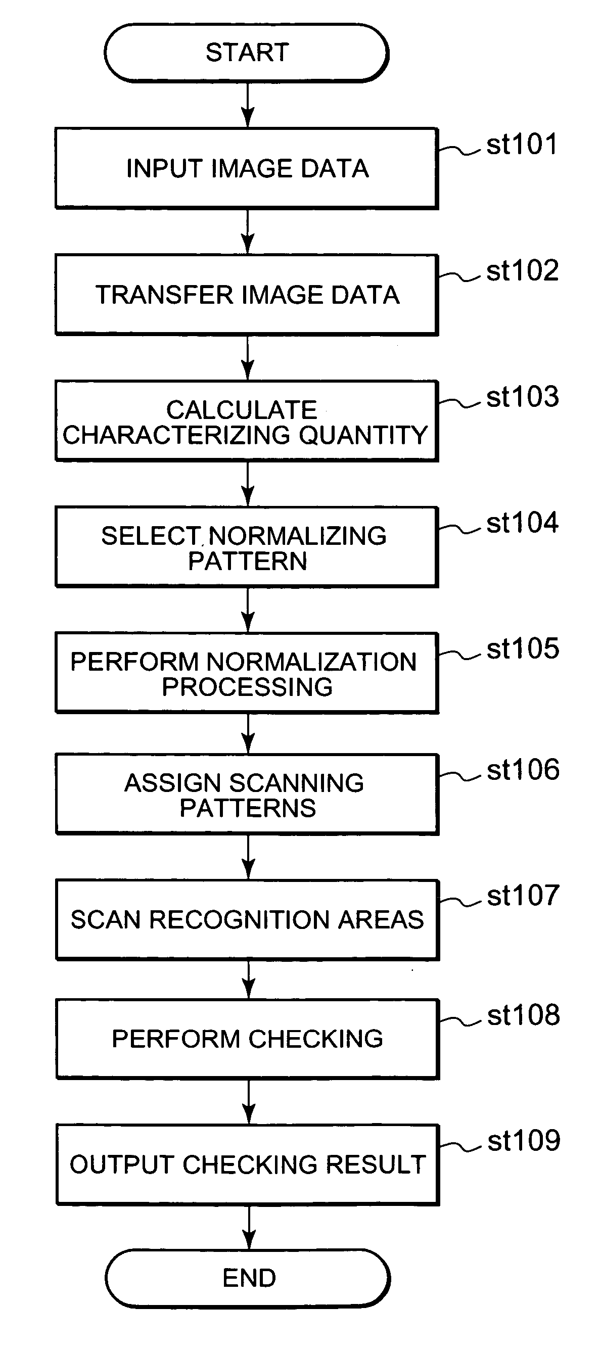
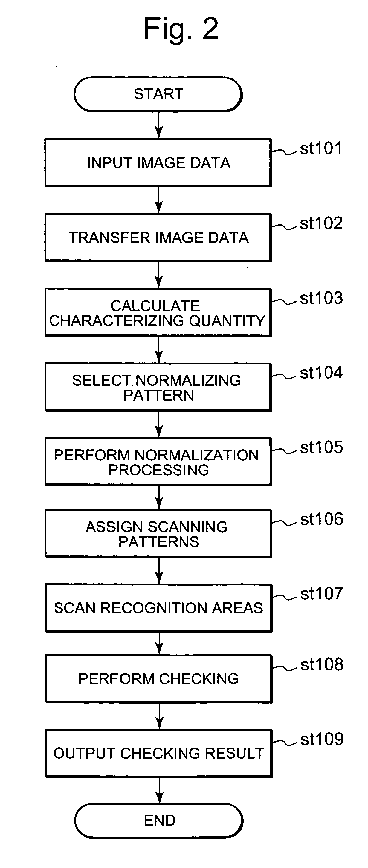
[0022]FIG. 1 is a block diagram of an image recognition device in Embodiment 1 for implementing the present invention. In FIG. 1, image data inputted to an input unit 1 by digitizing a video signal from an imaging device not shown in the figure is transferred to a feature quantity calculating unit 2 and to a normalization processing unit 4. The feature quantity calculating unit 2 calculates a feature quantity such as the mean or the variance of all pixel values of the image data frame by frame, and transfers the feature quantity to a normalizing pattern selecting unit 3. In a normalizing pattern recording unit 8, a look-up table including a plurality of kinds of normalizing patterns is recorded. The normalizing pattern selecting unit 3 refers to the look-up table recorded in the normalizing pattern recording unit 8, and selects a normalizing pattern that corresponds to the feature quantity calculated by the feature quantity calculating unit 2, to develop the normalizing pattern in a...

embodiment 2

[0041]FIG. 8 is a block diagram for an image recognition device in Embodiment 2 to implement the present invention, and identical numerals are attached to components corresponding to those in FIG. 1. In FIG. 8, image data inputted to the input unit 1 is transferred to the scanning unit 5 and an accumulated-image-data calculating unit 10. A scanning pattern assigning unit 6 assigns for each frame a scanning pattern in the scanning pattern recording unit 9, and the scanning unit scans recognition areas based on the assigned scanning pattern. In addition, the accumulated-image-data calculating unit 10 calculates accumulated image data from the image data for each frame. The feature quantity calculating unit 2 calculates feature quantities for the image data in a recognition area using the accumulated image data. The normalizing pattern selecting unit 3 refers to the look-up table recorded in the normalizing pattern recording unit 8, and selects a normalizing pattern corresponding to th...


PUM


Abstract

In order to reduce the computational burden required for scanning and to enhance the recognition accuracy, an image recognition device is configured so that a scanning pattern recording unit that records a plurality of scanning patterns for directing how to scan recognition areas of predetermined size in the image data is included, and different scanning patterns for successive frames are read out from the scanning pattern recording unit and applied to scan the recognition areas.

Description

BACKGROUND OF THE INVENTION [0001] 1. Field of the Invention [0002] The present invention relates to an image recognition device for performing recognition processes to detect presence of a target object. [0003] 2. Description of the Related Art [0004] In a conventional image recognition device, in order to speed up its recognition processes by skipping pixels in image data, the number of pixels skipped in the recognition processes, which is referred to as the skipping distance hereinafter, is configured in accordance with the size of a recognition target, and an image in a recognition area has been scanned with the configured skipping distance (see, for instance, Japanese Patent Laid-Open No. 99724 / 2000 (FIG. 2)). [0005] In addition, in the conventional image recognition device, in order to enhance detection-accuracy tolerance to luminance variations, a normalization process such as luminance tone adjustment is performed on the whole image or the recognition area within the image d...

Claims


Application Information

Patent Timeline
Patent Type & Authority Applications(United States)
IPC IPC(8): G06K9/00G06V10/22
CPCG06K9/2054G06V10/22
Inventor TANAKA, SHOJIOTSURU, MAKOTO
Owner MITSUBISHI ELECTRIC CORP
Why Eureka
Try Eureka