Adhesive system for supporting thin silicon wafer

a technology of adhesive system and silicon wafer, which is applied in the direction of basic electric elements, electrical apparatus, semiconductor devices, etc., can solve the problems of increasing the likelihood that the wafer may be damaged, the process of separating the silicon wafer from the carrier can be quite time-consuming and inefficien

Inactive Publication Date: 2007-04-05
INTEL CORP
View PDF2 Cites 35 Cited by
  • Summary
  • Abstract
  • Description
  • Claims
  • Application Information

AI Technical Summary

Problems solved by technology

However, backside processing tends to negatively affect the strength and rigidity of the wafer, thus increasing the likelihood that the wafer may be damaged through breakage or warping, especially where the wafer has a thickness below about 300 microns.
The process of subsequently separating the silicon wafer from the carrier can be quite time consuming and inefficient.

Method used


Image

  • Adhesive system for supporting thin silicon wafer
  • Adhesive system for supporting thin silicon wafer
  • Adhesive system for supporting thin silicon wafer

Examples


Embodiment Construction

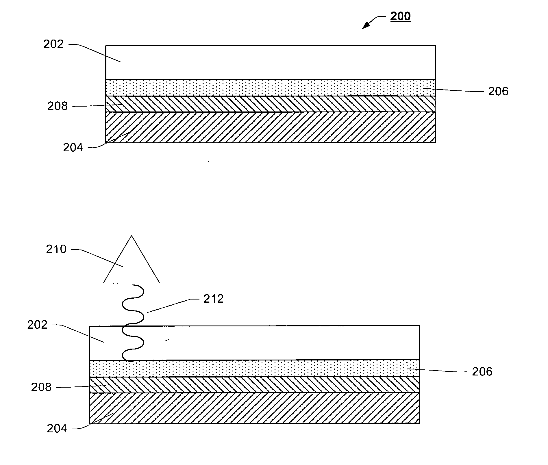
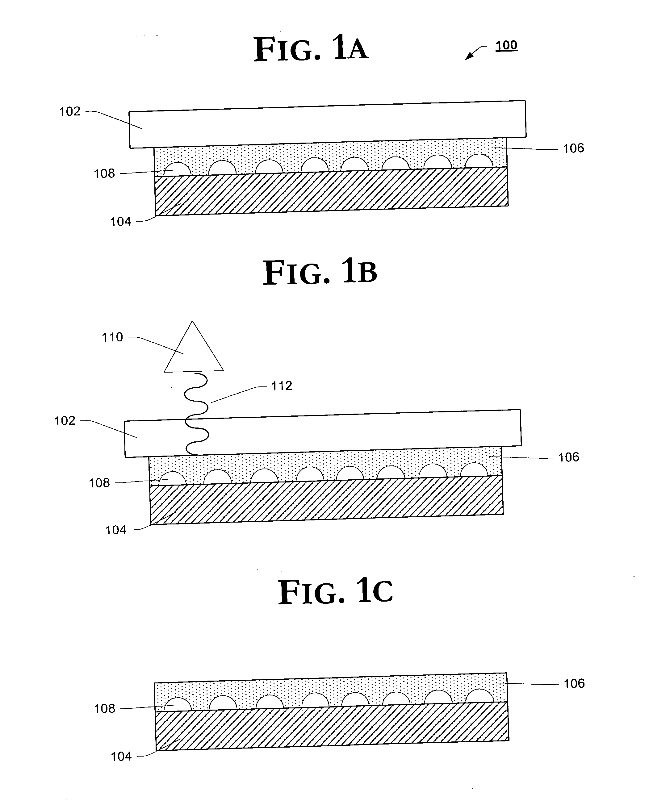
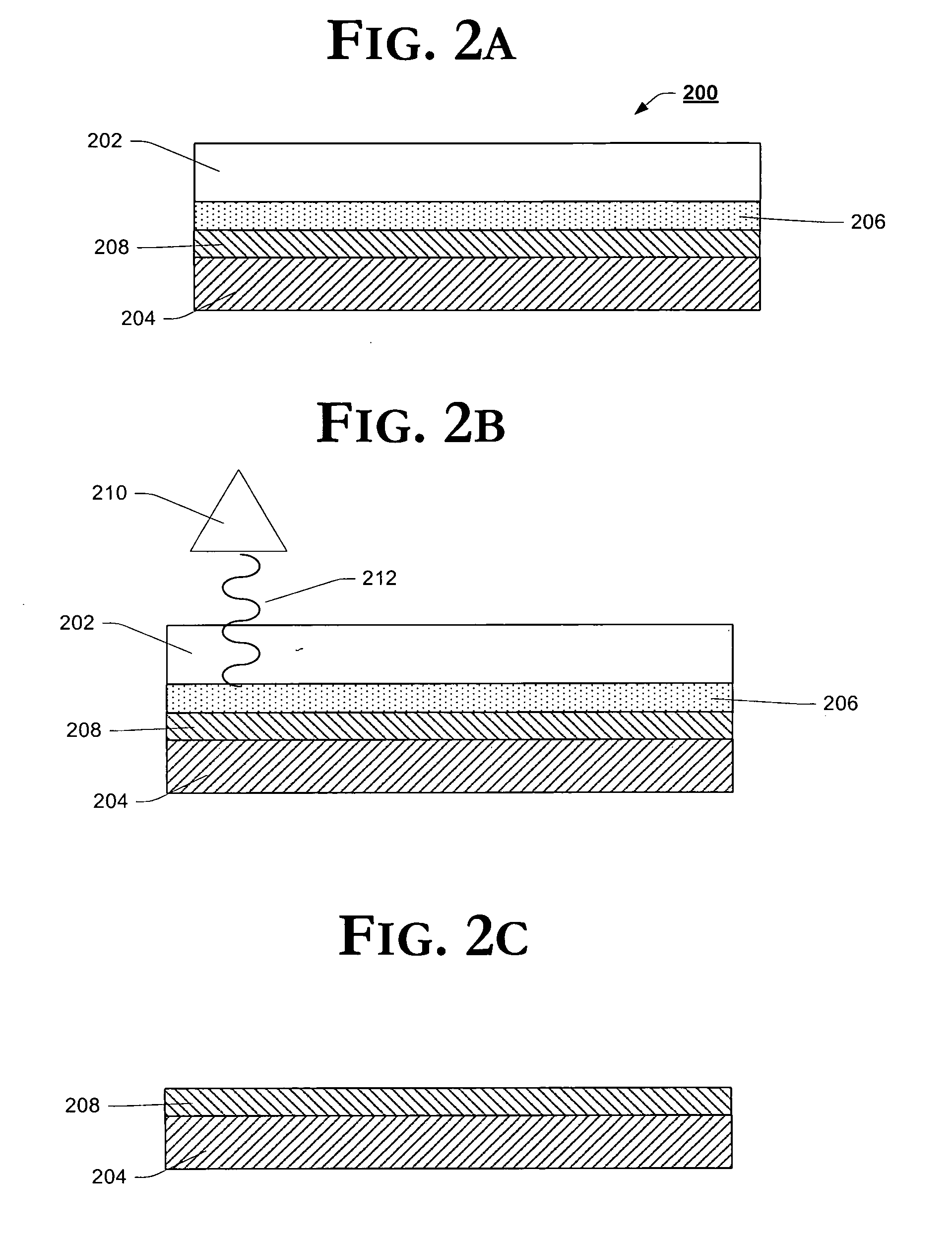
[0006] In the following description, for purposes of explanation, numerous specific details are set forth in order to provide a thorough understanding of the invention. It will be apparent, however, to one skilled in the art that embodiments of the invention can be practiced without these specific details. In other instances, structures and devices are shown in block diagram form in order to avoid obscuring the invention.

[0007] Reference throughout this specification to “one embodiment” or “an embodiment” means that a particular feature, structure or characteristic described in connection with the embodiment is included in at least one embodiment of the present invention. Thus, appearances of the phrases “in one embodiment” or “in an embodiment” in various places throughout this specification are not necessarily all referring to the same embodiment. Furthermore, the particular features, structures or characteristics may be combined in any suitable manner in one or more embodiments....


PUM


Abstract

In some embodiments, an adhesive system for supporting thin silicon wafer is presented. In this regard, a method is introduced to bond a silicon wafer to a translucent carrier through the use of an adhesive. Other embodiments are also disclosed and claimed.

Description

FIELD OF THE INVENTION [0001] Embodiments of the present invention generally relate to the field of processing silicon wafers, and, more particularly to an adhesive system for supporting thin silicon wafer. BACKGROUND OF THE INVENTION [0002] In the process of fabricating a microelectronic wafer (hereinafter “wafer”), backside processing is performed generally after a wiring pattern is provided on the front surface of the wafer. Backside processing may include mechanical or chemical methods for thinning the wafer, such as, for example, grinding, chemical-mechanical polishing, and etching. Backside processing may further include processes other than thinning, such as, for example, thin film deposition and / or electroplating. However, backside processing tends to negatively affect the strength and rigidity of the wafer, thus increasing the likelihood that the wafer may be damaged through breakage or warping, especially where the wafer has a thickness below about 300 microns. In order to...

Claims


Application Information

Patent Timeline
Patent Type & Authority Applications(United States)
IPC IPC(8): H01L21/30H01L21/46
CPCH01L21/78H01L21/6835H01L2221/68327H01L2221/6834H01L2221/68381
Inventor KULKARNI, SUDHAKAR N.ARANA, LEONEL R.PRACK, EDWARD R.
Owner INTEL CORP
Why Eureka
Try Eureka