Program method of flash memory device

a flash memory and program technology, applied in the field of flash memory devices, can solve the problems of negative effect on the reliability of cell operation and extended program time, and achieve the effect of reducing the threshold voltage distribution

Active Publication Date: 2007-04-12
SK HYNIX INC
View PDF5 Cites 63 Cited by
  • Summary
  • Abstract
  • Description
  • Claims
  • Application Information

AI Technical Summary

Benefits of technology

[0009] An embodiment of the present invention provides a program method of a flash memory device, in which the threshold voltage distribution can be reduced by applying a dummy pulse to a MLC having a state “10” at which a threshold voltage width is wide before the ISPP program operation.

Problems solved by technology

This has a negative effect on the reliability of cell operation.
Accordingly, a problem arises because the program time is lengthened.

Method used


Image

  • Program method of flash memory device
  • Program method of flash memory device
  • Program method of flash memory device

Examples


Embodiment Construction

[0018] The present invention will be described in detail in connection with certain embodiments with reference to the accompanying drawings. To clarify multiple layers and regions, the thickness of the layers is enlarged in the drawings.

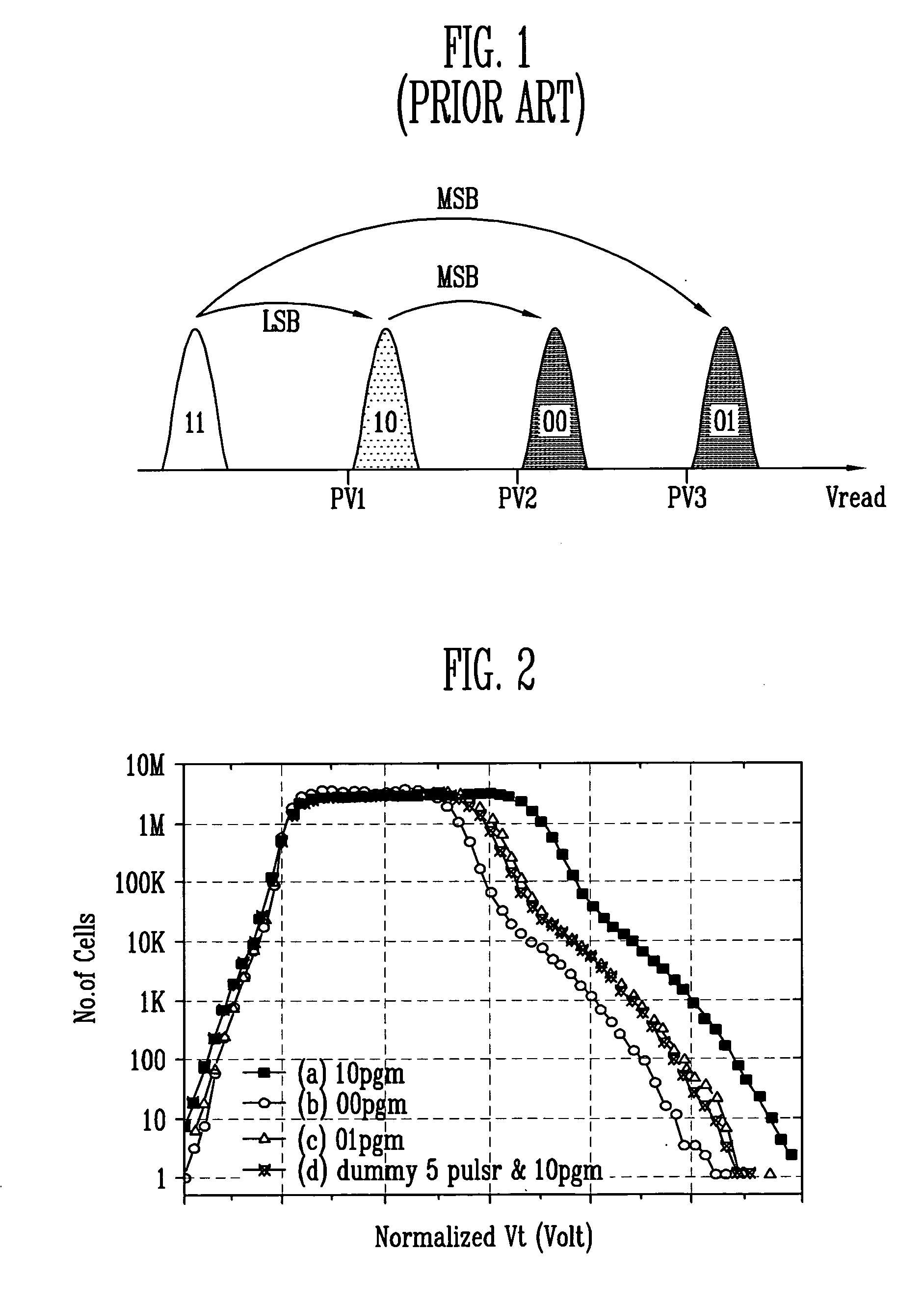
[0019]FIG. 2 is a graph in which respective program verify operations are moved to 0V in order to relatively compare the threshold voltage distributions with the program states “10”, “00”, and “01”. From FIG. 2, it can be seen that the threshold voltage distribution (b) of “00” is the narrowest and the threshold voltage distribution (a) of “10” is the widest.

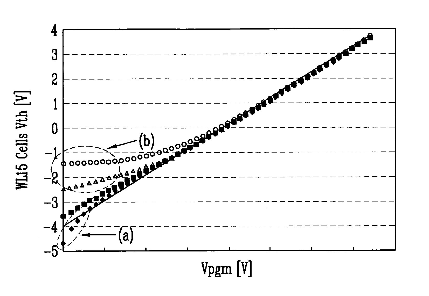
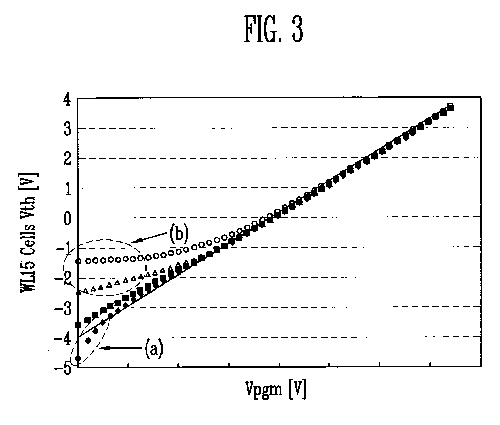
[0020] From FIG. 3, it can be seen that after the ISPP program operation is sufficiently performed, a constant threshold voltage is obtained regardless of an initial threshold voltage value of a cell, but while an initial ISPP program operation is carried out, variation in the threshold voltage by ISPP is different depending on the initial threshold voltage of the cell though program is perform...


PUM


Abstract

A method for programming a non-volatile memory device includes applying a first dummy voltage to a Multi-Level Cell (MLC). A first program voltage is applied to the MLC to program the MLC, the first program voltage being applied to the MLC after the first dummy voltage has been applied to the MLC. The MLC is verified whether or not the MLC has been programmed correctly by the first program voltage. A second dummy voltage is applied to the MLC after the first dummy voltage has been applied, the second dummy voltage being N volt higher than the first dummy voltage, wherein the second dummy voltage applied to the MLC is of sufficiently low voltage, so that the second dummy voltage does not change an initial state of the MLC. A third dummy voltage is applied to the MLC after the second dummy voltage has been applied, the third dummy voltage being N volt higher than the second dummy voltage.

Description

BACKGROUND [0001] The present invention relates to a flash memory device, and more particularly, to a program method which can reduce the threshold voltage distribution width of a flash memory device having a multi-level cell. [0002] Currently, there is an increasing demand for semiconductor memory devices which can be electrically programmed and erased and does not require refreshing the data. Furthermore, to develop large capacity memory devices, there has been research done to increase the level of integration. Accordingly, there has been much research done into flash memories. [0003] Flash memory is generally classified as NAND flash memory or NOR flash memory. The NOR flash memory has a structure in which memory cells are independently connected to bit lines and word lines. Its main advantage is a faster random access time. Meanwhile, the NAND flash memory has a structure in which a plurality of memory cells are connected in series and only one contact per cell string is requir...

Claims


Application Information

Patent Timeline
Patent Type & Authority Applications(United States)
IPC IPC(8): G11C11/34
CPCG11C11/5628G11C16/10
Inventor JOO, SEOK JIN
Owner SK HYNIX INC
Why Eureka
Try Eureka