Flash memory device and method for fabricating the same

a memory device and flash memory technology, applied in the field of flash memory devices, can solve the problems of increasing the threshold voltage distribution of the programming state in the entire device, increasing the distance between the cells, and increasing the probability of interference caused by the capacitance existing between the cells, so as to reduce the threshold voltage distribution and reduce the capacitance

Inactive Publication Date: 2007-06-07
SK HYNIX INC
View PDF4 Cites 10 Cited by
  • Summary
  • Abstract
  • Description
  • Claims
  • Application Information

AI Technical Summary

Benefits of technology

[0014] It is, therefore, an object of the present invention to provide a flash memory device capable of decreasing a threshold voltage distribution by reducing capacitance between adjacent floating gates and a method for fabricating the same.

Problems solved by technology

Thus, the distance between the cells decreases, and as a result, interference caused by the capacitance existing between the cells is more likely to occur.
Particularly, depending on a state of the peripheral cells, a programming state of the target cell is being affected, resulting in an increase of the threshold voltage distribution of the programming state in the entire device.
Particularly, with respect to the direction from the bit line to the bit line, the interference may increase due to capacitance between polysilicon layers.
However, in a structure obtained using the typical SA-STI process, enlarging the distance between the polysilicon layers often causes the area of an active region to be decreased.

Method used


Image

  • Flash memory device and method for fabricating the same
  • Flash memory device and method for fabricating the same
  • Flash memory device and method for fabricating the same

Examples


Embodiment Construction

[0022] Hereinafter, embodiments of the present invention will be described in detail with reference to the accompanying drawings.

[0023]FIG. 3 is a cross-sectional view illustrating a structure of a flash memory device in accordance with an embodiment of the present invention.

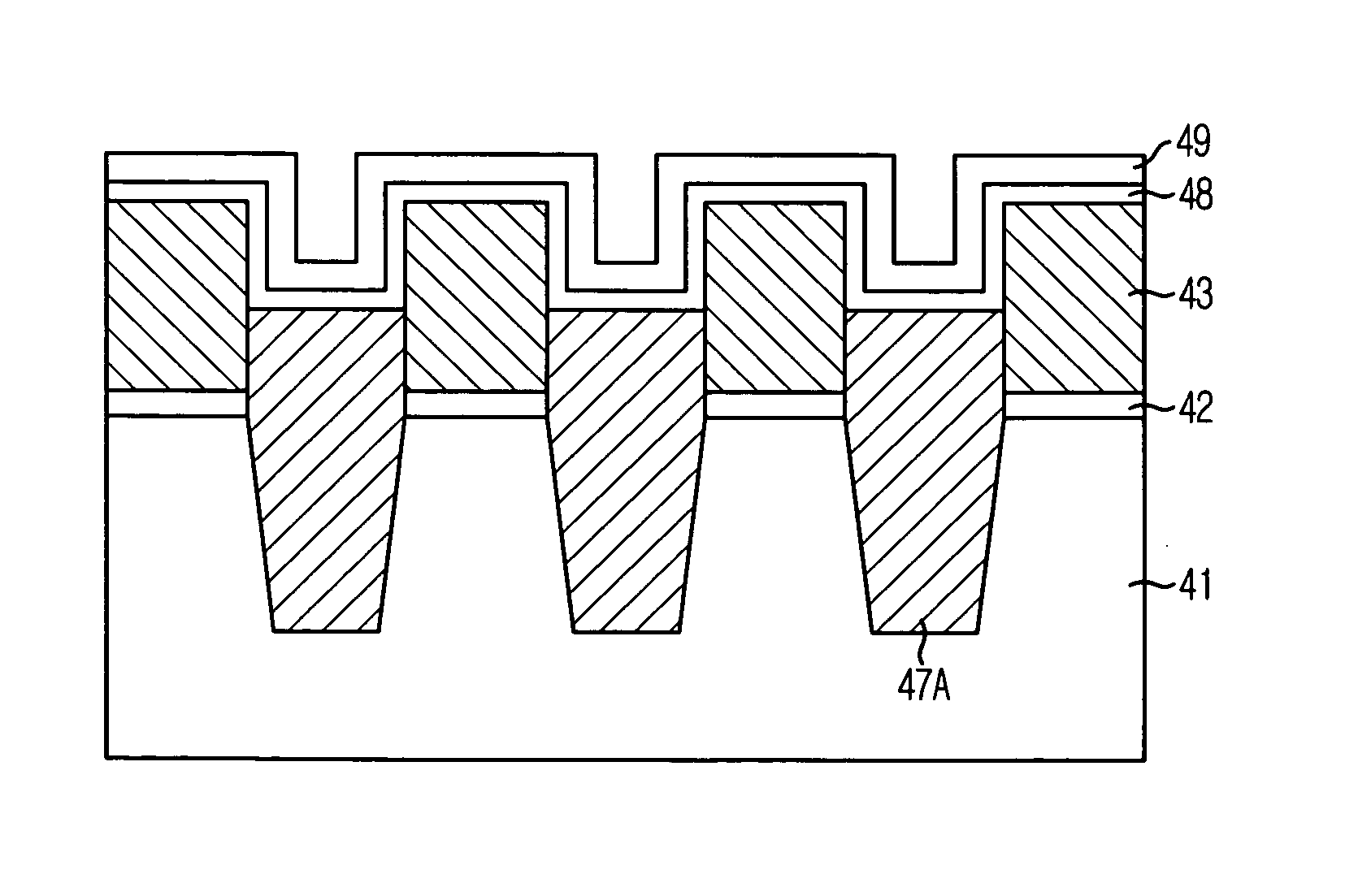
[0024] As illustrated, floating gates 33 are formed over certain regions of a substrate 31, and a tunnel oxide layer 32 is formed beneath the floating gates 33. Separated isolation layers 37A are formed in regions of the substrate 31 beneath the sidewalls of the floating gates 33. Trenches 40 are formed individually in top central portions of the separated isolation layers 37A. A dielectric layer 41 is formed over the floating gates 33 and the separated isolation layers 37A, and a control gate 42 is formed over the dielectric layer 41.

[0025] The floating gates 33 are formed to a thickness ranging from approximately 800 Å to approximately 1,200 Å. The dielectric layer 41 is formed in a structure of oxide / nitri...


PUM


Abstract

A flash memory device and a method for fabricating the same are provided. The method includes: preparing a semi-finished substrate where floating gates and an isolation layer isolating the floating gates are formed; recessing a predetermined portion of the isolation layer to make the floating gates protrude; etching another predetermined portion of the isolation layer to form a trench therein; forming a dielectric layer over the isolation layer and the floating gates; and forming a control gate over the dielectric layer such that the control gate fills the trench.

Description

FIELD OF THE INVENTION [0001] The present invention relates to a semiconductor memory device and a method for fabricating the same; and more particularly, to a flash memory device and a method for fabricating the same. DESCRIPTION OF RELATED ARTS [0002] In a flash memory device, as a cell threshold voltage distribution becomes narrow, program operation becomes faster and is increasingly advantageous in respect of reliability. In flash memory devices, capacitance exists between cells, and as the device size becomes smaller, the cell size also becomes smaller. Thus, the distance between the cells decreases, and as a result, interference caused by the capacitance existing between the cells is more likely to occur. This fact further causes a threshold voltage distribution of a programmed cell to become wide. [0003] During cell operation, if peripheral cells are programmed, the interference causes a threshold voltage of the programmed peripheral cells to increase to a greater extent as c...

Claims


Application Information

Patent Timeline
Patent Type & Authority Applications(United States)
IPC IPC(8): H01L21/336H01L29/76
CPCH01L21/76232H01L27/115H01L27/11521H10B69/00H10B41/30H10B43/30
Inventor CHO, JUNG-II
Owner SK HYNIX INC
Why Eureka
Try Eureka