Supercharge Your Innovation With Domain-Expert AI Agents!

Wafer structure with mirror shot

a technology of mirror shot and wafer, which is applied in the direction of instruments, semiconductor/solid-state device details, optical radiation measurement, etc., can solve the problems of increased probability of generating defects during die attachment operation, and poor die attachment performed based on the first die coordinate may be defective, so as to avoid a die attachment defect and stable die attachment

Active Publication Date: 2007-04-26
SAMSUNG ELECTRONICS CO LTD
View PDF4 Cites 0 Cited by
  • Summary
  • Abstract
  • Description
  • Claims
  • Application Information

AI Technical Summary

Benefits of technology

[0008] To solve the above and / or other problems, the present invention provides a wafer structure which enables stable die attachment while avoiding a die attachment defect.

Problems solved by technology

As wafer sizes increase and become thin, inking is omitted and accordingly a probability of generation of defects during the die attachment operation increases.
However, since there is no specific reference in recognition of the first die, an error can occur in the coordinate of the first die so that the good die attachment performed based on the first die coordinate may be defective.

Method used


Image

  • Wafer structure with mirror shot
  • Wafer structure with mirror shot
  • Wafer structure with mirror shot

Examples


Embodiment Construction

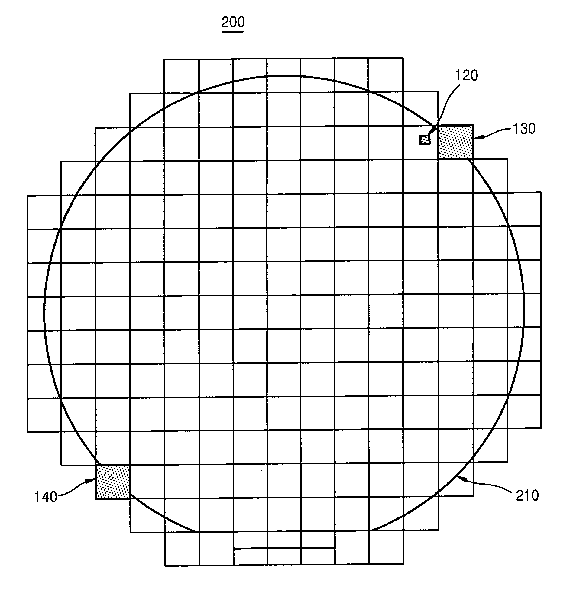
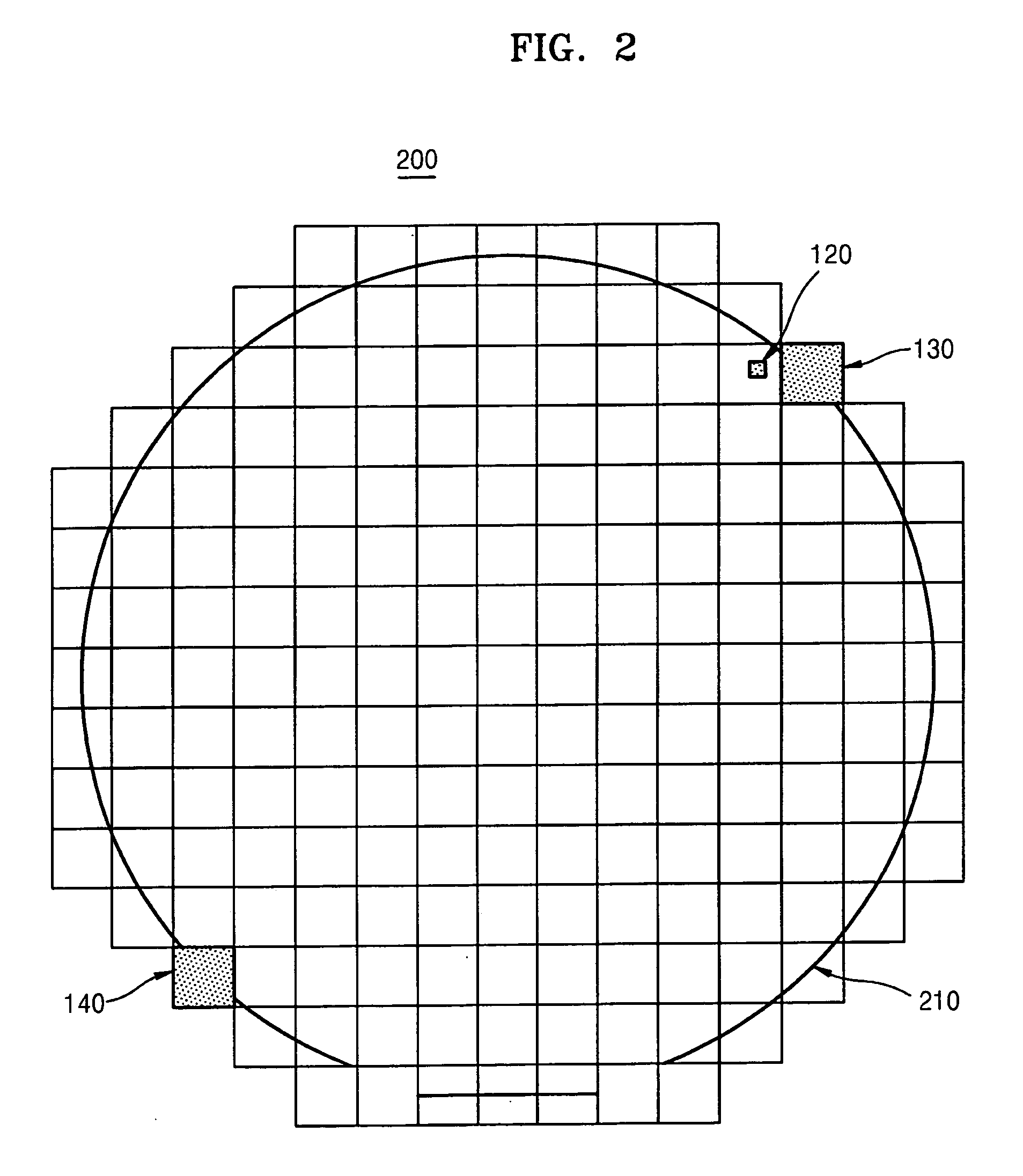
[0023]FIG. 1 is a view showing a wafer structure according to an embodiment of the present invention. In the wafer structure 100 of FIG. 1, wafer 110 is a notch wafer. However, according to the invention other types of wafer may be used in the wafer structure 100 of FIG. 1. Referring to FIG. 1, a wafer structure 100 according to an embodiment of the present invention includes a first mirror shot area 130 to which a mirror shot is applied. The position of a first die 120 is searched for based on the first mirror shot area 130.

[0024] The first die 120 is a die used as a reference coordinate in attaching a good die. A wafer structure 100 of FIG. 1 may further include a second mirror shot area 140 to which a mirror shot is applied. The first die 120 may be located in proximity to or at a portion adjacent to the first mirror shot area 130 as shown, and the first mirror shot area 130 and the second mirror shot area 140 may be diagonally located with respect to each other, as shown. Altho...


PUM


Abstract

A wafer structure with mirror shot is provided. A wafer structure according to the present invention comprises a first mirror shot area to which a mirror shot is applied, wherein the position of a first die is searched for based on the first mirror shot area. The wafer structure further comprises a second mirror shot area to which the mirror shot is applied. The second mirror shot area is located diagonally with respect to the first mirror shot area.

Description

CROSS-REFERENCE TO RELATED PATENT APPLICATIONS [0001] This application claims the benefit of Korean Patent Application No. 10-2005-0099617, filed on Oct. 21, 2005, in the Korean Intellectual Property Office, the contents of which are incorporated herein in their entirety by reference. BACKGROUND OF THE INVENTION [0002] 1. Field of the Invention [0003] The present invention relates to a wafer structure, and more particularly, to a wafer structure in which a mirror shot is performed for a partial area of a wafer for stable die attachment. [0004] 2. Description of the Related Art [0005] For semiconductor circuit devices that are assembled after a test is completed, a good die and a bad die are accurately classified only by recognition of the presence of inking, and die attachment is performed only for the good die. The inking is performed to classify a good die and a bad die by marking a surface of each die using ink. As wafer sizes increase and become thin, inking is omitted and accor...

Claims


Application Information

Patent Timeline
Patent Type & Authority Applications(United States)
IPC IPC(8): G01B11/28G01J3/28
CPCH01L21/67294H01L21/68H01L21/50
Inventor KIM, YOUNG-DAEKIM, DAE-YOUNG
Owner SAMSUNG ELECTRONICS CO LTD
Features
  • R&D
  • Intellectual Property
  • Life Sciences
  • Materials
  • Tech Scout
  • Unparalleled Data Quality
  • Higher Quality Content
  • 60% Fewer Hallucinations
Learn More