Methods, Apparatus and Computer Program Products for Generating Selective Netlists that Include Interconnection Influences at Pre-Layout and Post-Layout Design Stages

a technology of interconnection influences and netlists, applied in the field of circuit design units, can solve the problems of affecting the performance increasing design costs and design time, and difficult to change the parasitic resistance and parasitic capacitance of interconnections, so as to reduce the time required for simulation of semiconductor integrated circuits, accurately analyze the modeling of parasitic resistance and parasitic capacitance, and reduce the effect of designer errors

Inactive Publication Date: 2007-04-26
SAMSUNG ELECTRONICS CO LTD
View PDF25 Cites 26 Cited by
  • Summary
  • Abstract
  • Description
  • Claims
  • Application Information

AI Technical Summary

Benefits of technology

[0020] In some further embodiments of the present invention, cells and interconnections for analyzing specific operations can be selected in the simulation schematic circuit including the parasitic resistance and parasitic capacitance of the interconnections. Accordingly, various simulations can be analyzed quite accurately, and the time required for the simulation of a semiconductor integrated circuit can be effectively reduced. Also, in the selective netlist generation device and the method therefor according to the present invention, the parasitic RC interconnections generated in a pre-layout step or in a post-layout step are generated as the schematic circuit and then interfaced in a simulation device. As a result, as compared to the case that the netlist of the parasitic RC interconnection is interfaced as a file in the simulation device, errors caused by the designer can be reduced. Also, the present invention allows the designer to accurately analyze modeling of the parasitic resistance and parasitic capacitance. Further, it becomes easier for the designer to insert a variety of simulation options into the schematic circuit.

Problems solved by technology

Thus, the designer could model only a part of the parasitic resistance and the parasitic capacitance of the interconnection, which greatly affect the performance of the semiconductor integrated circuit.
As a result, the work of designing the parasitic resistance and parasitic capacitance of the interconnection increases design costs and design time.
Also, when a floor plan, which is schematic layout information of a semiconductor integrated circuit, was changed, it was difficult to change the parasitic resistance and parasitic capacitance of the interconnection.
Therefore, in the pre-layout stage, it was difficult to perform a simulation on the semiconductor integrated circuit, considering the parasitic resistance and parasitic capacitance of the interconnection.
Thus, when the semiconductor integrated circuit was simulated, errors such as a convergence error occurred often.
Also, a lot of problems were caused when a control card was input or a probe sentence was inserted for analysis of the simulation results.
Also, connections needed to be inconveniently tracked from the netlist having file formats other than the schematic circuit during the analysis of the simulation results.
But, as the netlist input to the simulation device has a particular file format, if a schematic circuit is changed, the foregoing simulation method using the layout design unit may become inconvenient.
Besides, the simulation method is applied to the full-chip of the semiconductor integrated circuit, and this may require a large simulation time.

Method used


Image

  • Methods, Apparatus and Computer Program Products for Generating Selective Netlists that Include Interconnection Influences at Pre-Layout and Post-Layout Design Stages
  • Methods, Apparatus and Computer Program Products for Generating Selective Netlists that Include Interconnection Influences at Pre-Layout and Post-Layout Design Stages
  • Methods, Apparatus and Computer Program Products for Generating Selective Netlists that Include Interconnection Influences at Pre-Layout and Post-Layout Design Stages

Examples


Embodiment Construction

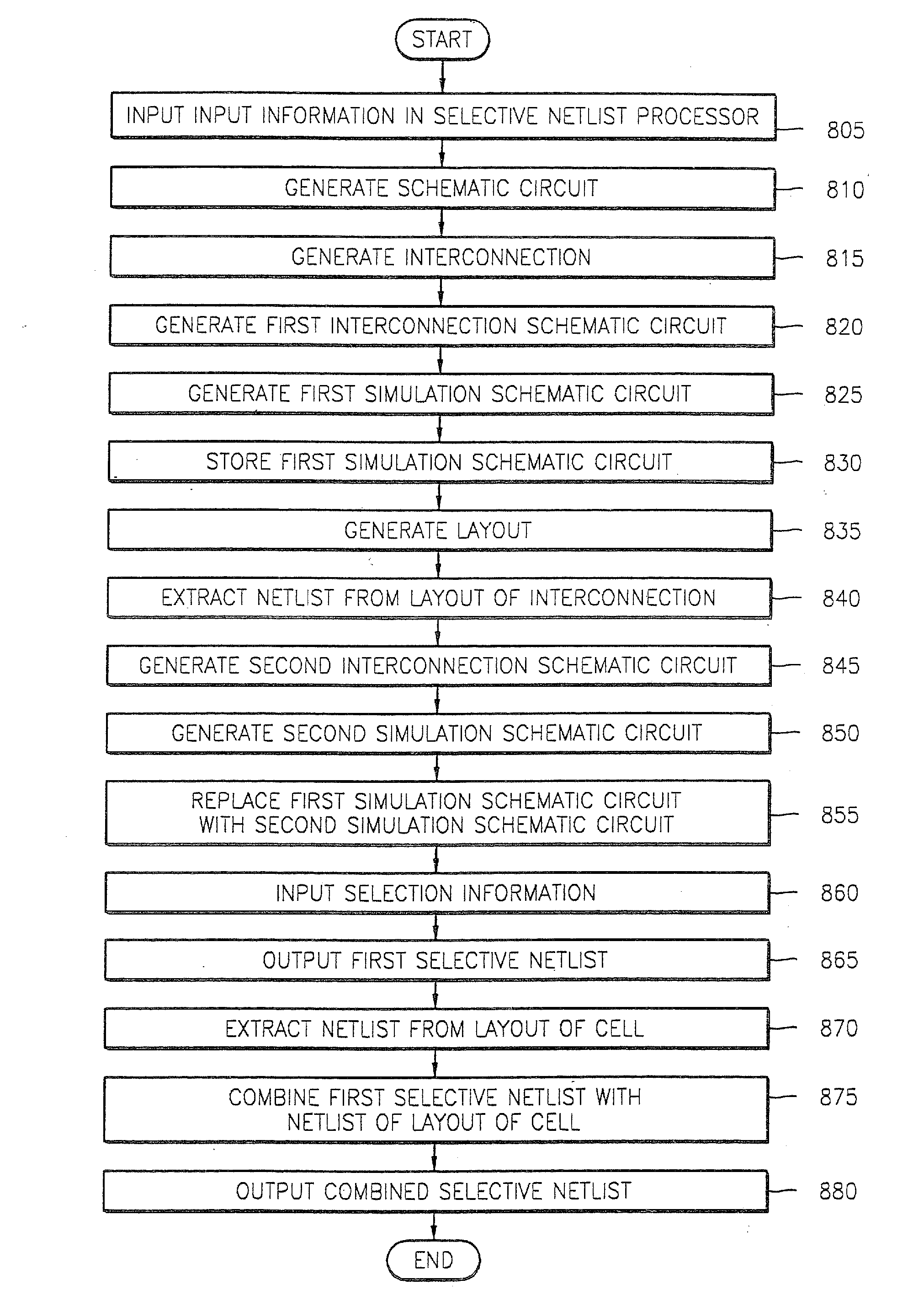
[0037] The structure and operation of each embodiment of a selective netlist generation device according to the present invention and a method according to the present invention for each embodiment of the selective netlist generation device will be described more fully with reference to the accompanying drawings, in which preferred embodiments of the invention are shown. The same reference numerals in different drawings represent the same element. The operations described hereinbelow may be performed by an entirely hardware embodiment, an entirely software embodiment or an embodiment combining software and hardware aspects. Moreover, embodiments of the invention may take the form of a computer program product on a computer-readable storage medium having computer-readable program code means embodied in the medium. Any suitable computer-readable medium may be utilized including hard disks, CD-ROMs or other optical or magnetic storage devices.

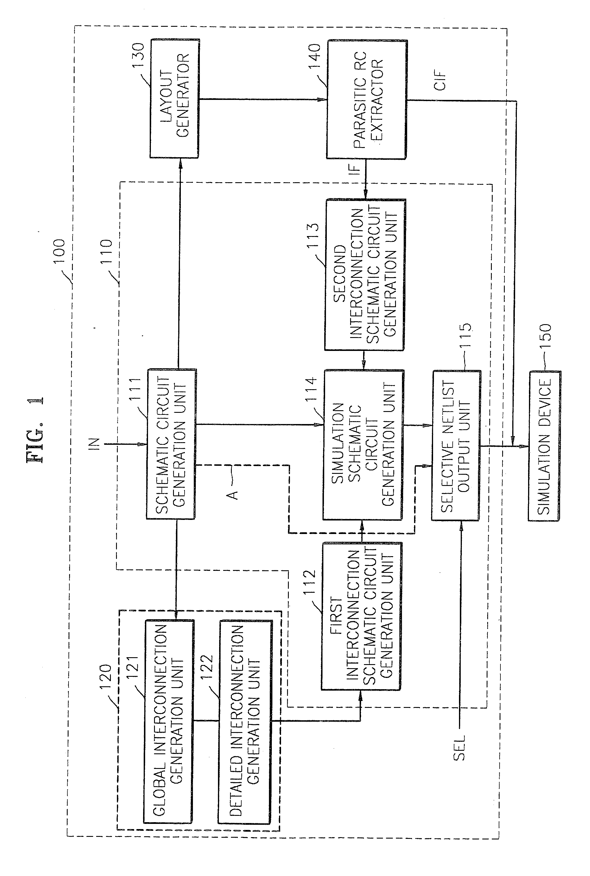
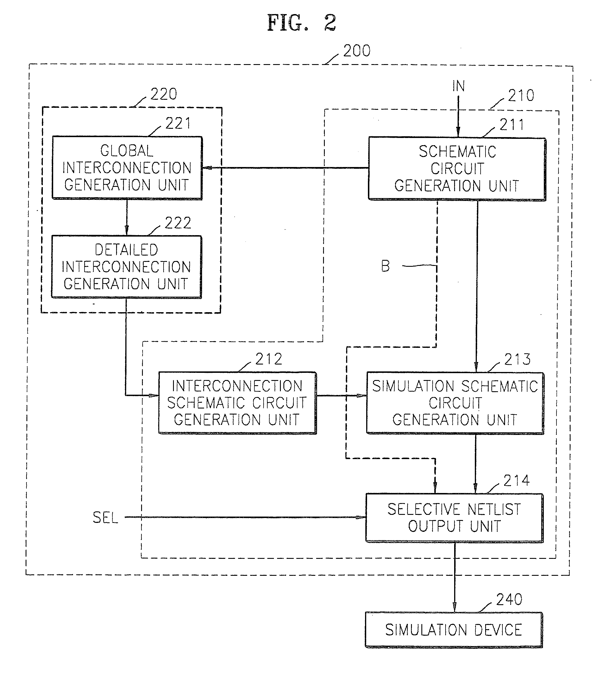
[0038]FIG. 1 is a block diagram illustrati...


PUM


Abstract

Operations for generating an integrated circuit netlist include generating a first schematic of an integrated circuit having a plurality of cells therein and generating a second schematic that defines pre-layout electrical interconnects between the plurality of cells of the integrated circuit and approximates parasitic resistances and parasitic capacitances of the pre-layout interconnects. The first and second schematics are then combined at corresponding first and second ports within the first and second schematics, respectively. Operations also include generating an integrated circuit netlist by generating a circuit schematic that defines post-layout electrical interconnects between the plurality of cells of the integrated circuit and approximates parasitic resistances and parasitic capacitances of the post-layout interconnects. This circuit schematic is then combined with the first schematic at corresponding first and second ports therein. These embodiments may also be configured to generate a layout schematic from the first schematic of the integrated circuit and generate parasitic resistances and capacitances of the post-layout interconnects that extend between a plurality of cells in the layout schematic. Operations are then performed to generate parasitic resistances and capacitances of interconnects internal to at least one cell in the layout schematic.

Description

REFERENCE TO PRIORITY APPLICATION [0001] This application is a divisional of U.S. application Ser. No. 10 / 629,154, filed Jul. 29, 2003, which claims priority to Korean Application No. 2002-76695, filed on Dec. 4, 2002. The disclosure of U.S. application Ser. No. 10 / 629,154 is hereby incorporated herein by reference.FIELD OF THE INVENTION [0002] The present invention relates to circuit design units, and more particularly, to devices for generating integrated circuit netlists that support device simulation. BACKGROUND OF THE INVENTION [0003] In general, the design of semiconductor integrated circuits follows a set method. To begin with, a schematic circuit, which is a diagram showing connections between circuit devices, can be designed by a schematic tool. Next, the respective circuit devices included in the schematic circuit can be designed by patterns of such material layers as a conductive layer, a semiconductor layer, and an insulation layer. Then, a layout is designed where the r...

Claims


Application Information

Patent Timeline
Patent Type & Authority Applications(United States)
IPC IPC(8): G06F17/50H01L21/82
CPCG06F17/505G06F17/5068G06F30/327G06F30/39
Inventor LEE, JONG-BAEYOO, MOON-HYUNKIM, KYO-SUNCHOI, JEONG-MIN
Owner SAMSUNG ELECTRONICS CO LTD
Why Eureka
Try Eureka