Semiconductor integrated circuit device, and debugging system and method for the semiconductor integrated circuit device

Active Publication Date: 2007-05-03
RENESAS ELECTRONICS CORP
View PDF12 Cites 17 Cited by
  • Summary
  • Abstract
  • Description
  • Claims
  • Application Information

AI Technical Summary

Benefits of technology

[0037] According to the debugging method, if a program execution of a predetermined processor satisfies a break condition, some of plural subsystems (processors or peripheral devices) can be stopped in sync wi

Problems solved by technology

For example, when the peripheral device operates in parallel to the CPU core, if the peripheral device is operating even though the CPU core is stopped, an internal condition of the CPU core or a memory is updated, making it difficult to check the internal condition correctly.
Further, if a break occurs, all CPU cores connected with the debugging synchronous bus are stopped all the time, and it is impossible to stop only a target CPU core.
However, since the debugging external bus is a low-speed bus, it takes much time for the debug PC to collect trace data from the DCU.
In general, a memor

Method used


Image

  • Semiconductor integrated circuit device, and debugging system and method for the semiconductor integrated circuit device
  • Semiconductor integrated circuit device, and debugging system and method for the semiconductor integrated circuit device
  • Semiconductor integrated circuit device, and debugging system and method for the semiconductor integrated circuit device

Examples


first embodiment

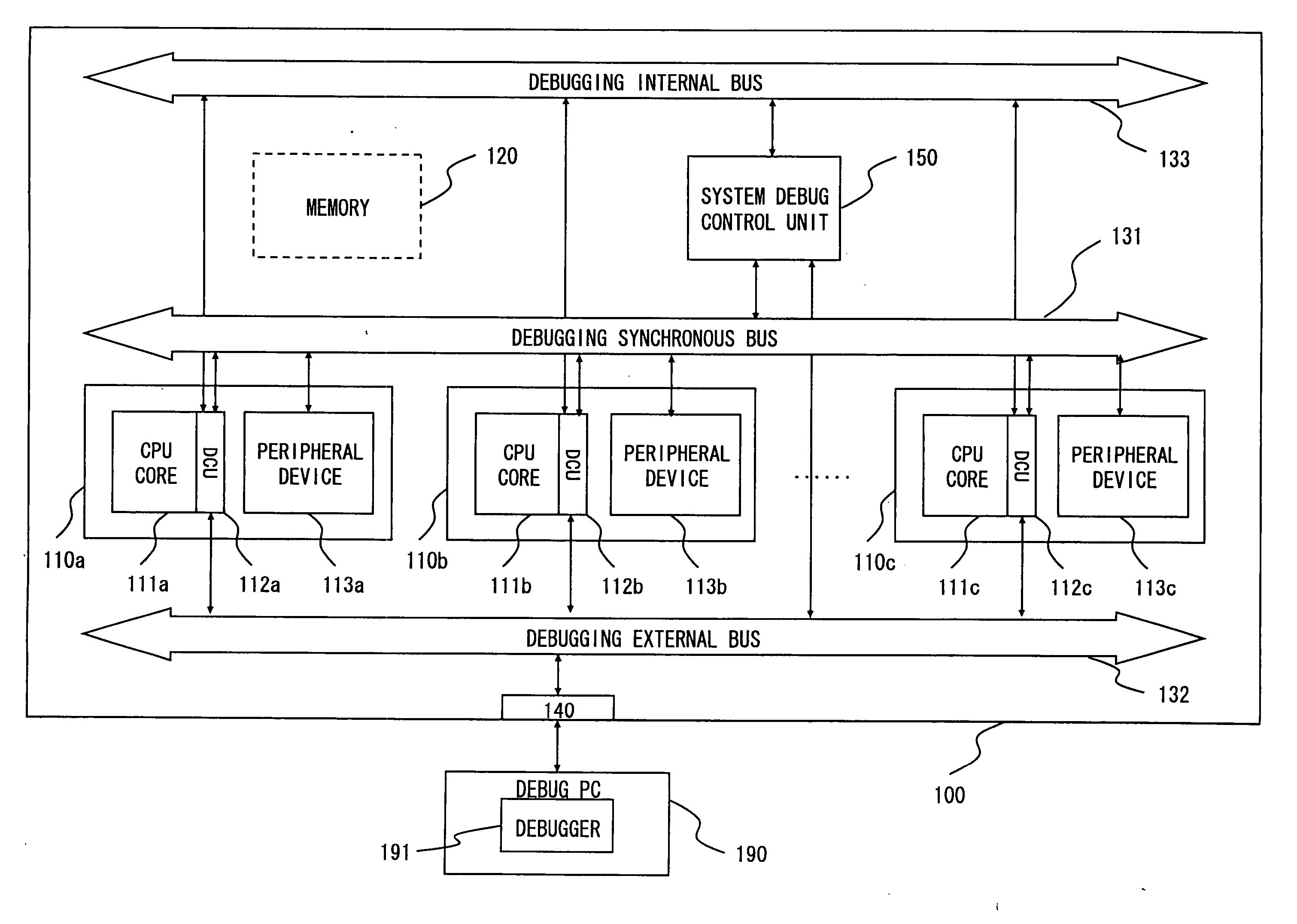
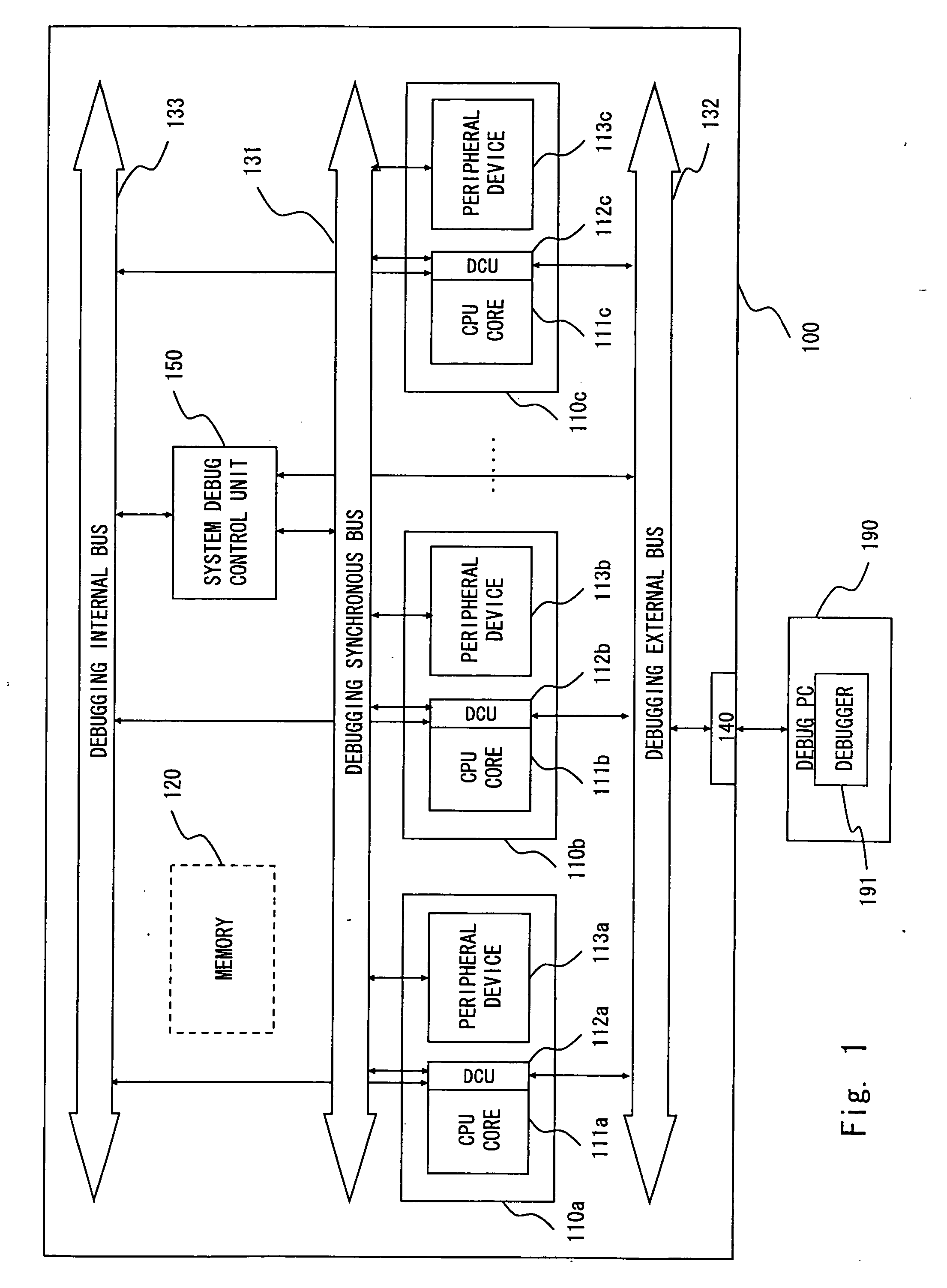
[0056] To begin with, a debugging system according to a first embodiment of the present invention is described. A feature of the debugging system of this embodiment is that a system debug control unit in an LSI controls synchronization when the break occurs, and plural trace data in each DCU are stored in the LSI.

[0057] Referring now to FIG. 1, the configuration of the debugging system of this embodiment is described. The debugging system is a system for debugging the LSI of multiprocessor configuration, and includes an LSI 100 and a debug PC 190. The LSI 100 and the debug PC 190 are connected through a debug I / F 140. The debug I / F 140 is a debug-only interface, for example, a low-speed serial interface such as a JTAG interface.

[0058] The debug PC 190 is made up of, for example, a computer such as a personal computer. The debug PC 190 includes a debugger 191 incorporating a debug control program. The LSI 100 is debugged in response to a user's manipulation on the debugger 191. The...


PUM


Abstract

To provide a debugging system, debugging method, and a semiconductor integrated circuit device capable of collecting debug-target information with accuracy and improving debug efficiency. A semiconductor integrated circuit device according to an embodiment of the present invention includes: subsystems; a break detecting unit detecting that a program execution of a CPU core in one subsystem satisfies a predetermined break condition; and a break selecting unit stopping operations of one selected from the subsystems in accordance with the detection result of the break detecting unit.

Description

BACKGROUND OF THE INVENTION [0001] 1. Field of the Invention [0002] The present invention relates to a semiconductor integrated circuit device, and a debugging system and method for the semiconductor integrated circuit device. In particular, the invention relates to a semiconductor integrated circuit device including a microprocessor, and a debugging system and method for debugging the same. [0003] 2. Description of Related Art [0004] In recent years, semiconductor integrated circuit devices (LSI) show a growing tendency to enhance the speed and performance of a built-in microprocessor. To that end, a semiconductor integrated circuit device of multiprocessor configuration which incorporates plural processors for attaining higher performance beyond the limit of the performance of a single microprocessor has been used. [0005]FIG. 12 shows a configuration example of a general LSI of multiprocessor configuration. As shown in FIG. 12, the LSI 800 includes plural subsystems (subsystems 81...

Claims


Application Information

Patent Timeline
IPC IPC(8): G06F11/00
CPCG06F11/3632G06F11/3636
Inventor UENO, SHIGEYUKI
Owner RENESAS ELECTRONICS CORP
Why Eureka
Try Eureka