Organic light emitting display device and driving method thereof

a technology of light-emitting display device and driving method, which is applied in the direction of static indicating device, electroluminescent light source, instruments, etc., can solve the problems of deteriorating yield, image sticking development, white balance variation, etc., and achieve the effect of shorter life time and longer yield

Active Publication Date: 2007-05-10
SAMSUNG DISPLAY CO LTD
View PDF13 Cites 33 Cited by
  • Summary
  • Abstract
  • Description
  • Claims
  • Application Information

AI Technical Summary

Benefits of technology

[0031] Accordingly, it is an aspect of the present invention to provide an organic light emitting display device and a driving method thereof, which solve problems due to variation between the life time durations of red, green, and blue organic light emitting diodes by using a time division control drive method for organic light emitting diodes having a relatively longer life time and by using a general drive method for organic light emitting diodes having a relatively shorter life time.

Problems solved by technology

According to a construction of the conventional organic light emitting display device, since each pixel includes three unit pixels, a plurality of wirings and a plurality of elements are arranged in every pixel, the circuit arrangement is complex, and it increases occurrence of defects, thereby deteriorating yield.
Accordingly, as time goes by, luminance reduction degrees are different in the R, G, and B unit pixels, thereby causing a white balance variation and an image sticking development.

Method used


Image

  • Organic light emitting display device and driving method thereof
  • Organic light emitting display device and driving method thereof
  • Organic light emitting display device and driving method thereof

Examples


Embodiment Construction

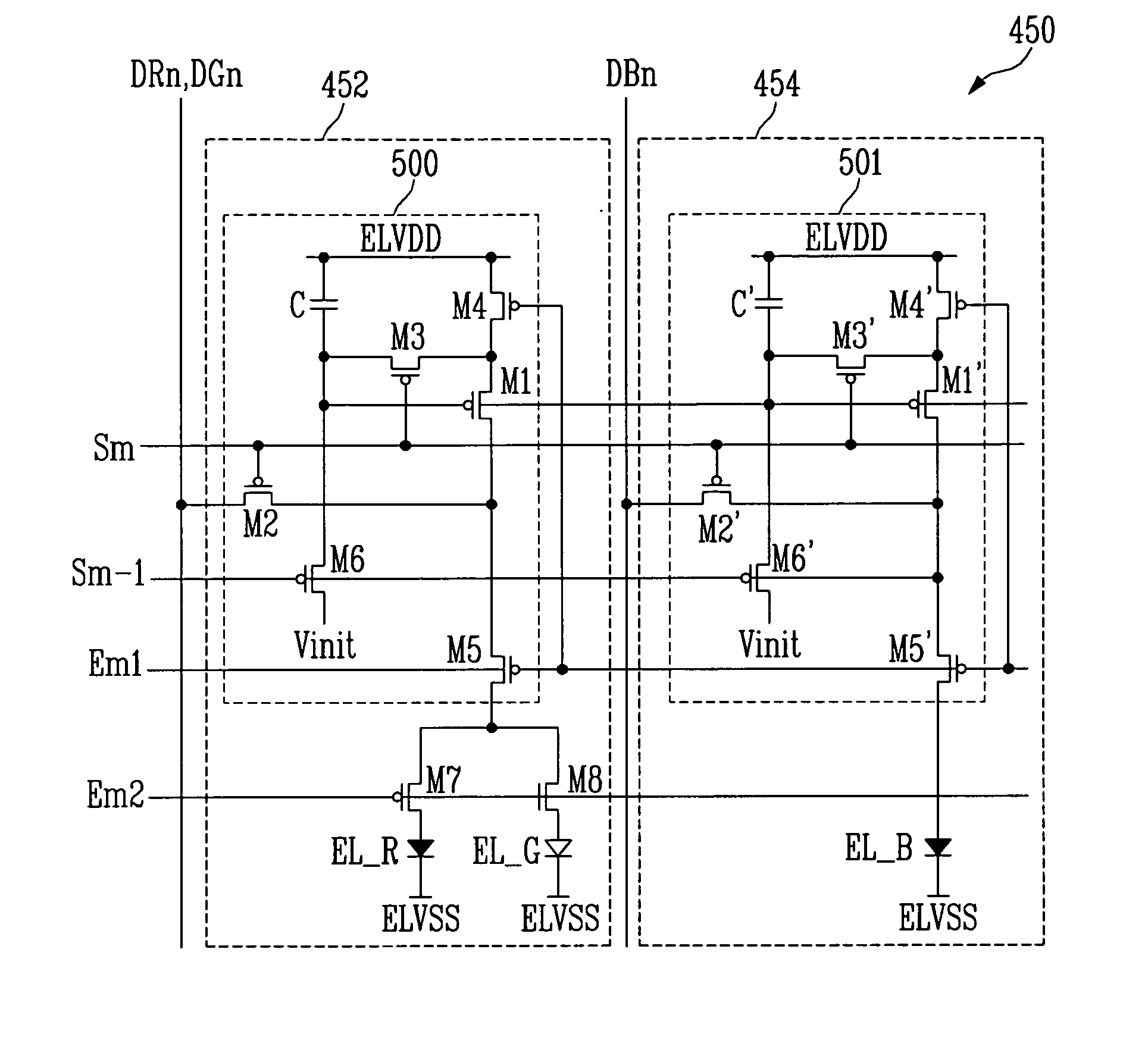
[0042] Hereinafter, exemplary embodiments according to the present invention will be described with reference to the accompanying drawings. Here, when one element is described to be connected to another element, the element may be directly connected to the other element or indirectly connected to the other element via one or more other elements. Further, some nonessential elements are omitted for clarity. Also, like reference numerals refer to like elements throughout.

[0043]FIG. 4 is a block diagram showing a configuration of an organic light emitting display device according to an embodiment of the present invention. The organic light emitting display device of FIG. 4 is one embodiment but the present invention is not limited thereto.

[0044] With reference to FIG. 4, the organic light emitting display device 400 according to an embodiment of the present invention includes a display region 410, a gate drive circuit 430, a data drive circuit 420, and an emission control signal gener...


PUM


Abstract

An organic light emitting diode (OLED) display device and a driving method using a time division control drive method for OLEDs having a relatively longer life time and a general drive method for OLEDs having a relatively shorter life time. A gate drive circuit provides scan signals in sub-frames to scan lines. A data drive circuit provides a data signal to data lines. An emission control signal generation circuit provides first and second emission control signals to control the OLEDs. A display region includes pixels arranged in a matrix and connected to the scan lines, data lines, emission control lines, and power lines. The pixels include a first and a second unit pixel portion. The first unit pixel portion performs a time division control drive by driving a plurality of organic light emitting diodes by one shared pixel circuit. In the second unit portion one organic light emitting diode is driven by an independent pixel circuit.

Description

CROSS-REFERENCE TO RELATED APPLICATION [0001] This application claims priority to and the benefit of Korean Patent Application No. 10-2005-0105699, filed on Nov. 4, 2005, in the Korean Intellectual Property Office, the entire content of which is incorporated herein by reference. BACKGROUND [0002] 1. Field of the Invention [0003] The present invention relates to an organic light emitting display device and a driving method thereof, and more particularly to an organic light emitting display device and a driving method thereof, which solve problems due to a life time variation of red, green, and blue organic light emitting diodes. [0004] 2. Discussion of Related Art [0005] Recently, since liquid crystal display devices and organic light emitting display devices have lightweight and thinness characteristics, they have been widely used in a field of portable information devices. In particular, since light emitting display devices have greater useful temperature range, higher resistance t...

Claims


Application Information

Patent Timeline
Patent Type & Authority Applications(United States)
IPC IPC(8): G09G3/30H05B44/00
CPCG09G3/3233G09G3/3291G09G2300/0443G09G2300/0452G09G2300/0465G09G2300/0814G09G2300/0861G09G2310/0235G09G2320/043G09G2300/0819G09G3/30H05B33/10
Inventor KWAK, WON KYUNAOAKI, KOMIYA
Owner SAMSUNG DISPLAY CO LTD
Why Eureka
Try Eureka