Low Bias Drift Modulator With Buffer Layer

a buffer layer and modulator technology, applied in the field of fiberoptic telecommunications optical devices, can solve the problems of weak electric fields loss of transmitted data, etc., and achieve the effects of reducing manufacturing and material costs, reducing substrate charging, and reliable operation

Active Publication Date: 2007-05-24
LUMENTUM OPERATIONS LLC
View PDF19 Cites 15 Cited by
  • Summary
  • Abstract
  • Description
  • Claims
  • Application Information

AI Technical Summary

Benefits of technology

[0026] In this way it is possible to operate the device with zero or nearly zero DC voltage between the highly conductive electrodes located on the surface of the device. As a result, metal migration and other effects which can cause electrode corrosion are mitigated, permitting reliable operation of the device in non-hermetic packages which are advantageous because of lower manufacturing and material costs.
[0027] Further, the electrodes located on the surface of the substrate, having an electrical connection to external terminals, can be used to eliminate substrate charging and similar effects, which would otherwise cause unstable device operation such as drift.
[0029] Another feature of the present invention provides for vias to connect the high resistivity bias electrodes to highly conducting electrodes to reduce the series resistance of the bias electrodes.

Problems solved by technology

Such strong electric fields are problematic because they can change the operating (bias) point of an electro-optic modulator, such as a Mach-Zehnder Interferometer (MZI), by creating fields across the waveguides that do not match one another.
In addition, these strong electric fields can cause time dependent or uncontrolled charge dissipation, which may result in a loss of transmitted data.
These fields may also cause arcing, which may also result in a loss of transmitted data.
A problem associated with LiNbO3 modulators is undesirable charge generation and charge redistribution that can occur when a bias voltage is applied to an electrical input of a LiNbO3 Mach-Zehnder interferometric modulator.
Positive drift is particularly problematic because the voltage required to maintain the bias condition will steadily increase (“run away”) causing a control system reset to occur, which will result in loss of data.
This separate bias electrode does not have a buffer layer between the electrode and substrate, eliminating problems associated with the buffer layer, however it increases the length of the device.
Note however that the bleed layer material is not patterned to form electrodes, nor does it provide a means to externally control the electric potential in the vicinity of the waveguides.

Method used


Image

  • Low Bias Drift Modulator With Buffer Layer
  • Low Bias Drift Modulator With Buffer Layer
  • Low Bias Drift Modulator With Buffer Layer

Examples


Embodiment Construction

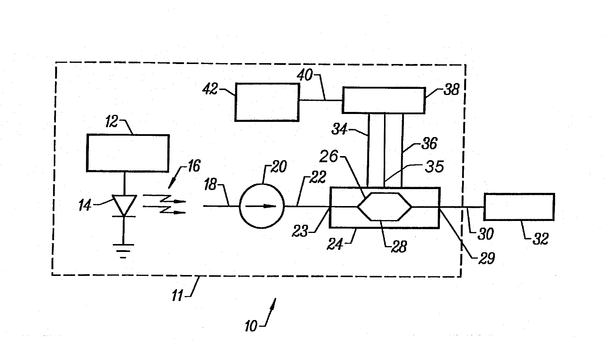
[0075] With reference to FIG. 1, an embodiment of a simplified optical communication system 10 is shown, utilizing a modulator 24 of the present invention. The optical communication system 10 comprises a transmitter 11, a receiver 32 and a transmission medium 30, which connects the transmitter 11 to the receiver 32. The transmission medium 30 is typically an optical fiber.

[0076] The transmitter 11 includes a laser 14, which operates in accordance with laser control signals received from a laser controller 12. The laser 14, which may operate in continuous wave (CW) mode or pulsed mode, produces optical signals 16 having a prescribed wavelength. In long wavelength communications systems, the laser 14 is typically an InGaAsP / InP semiconductor single-mode laser which generates 1.5 micrometer wavelength optical signals.

[0077] A lensed optical fiber 18, or fiber pigtail, receives the optical signals 16. The lensed optical fiber 18 is coupled to the isolator 20, which reduces reflections...


PUM


Abstract

The invention relates to an electro-optic modulator structure containing an additional set of bias electrodes buried within the device for applying bias to set the operating point. Thus the RF electrodes used to modulate incoming optical signals can be operated with zero DC bias, reducing electrode corrosion by galvanic and other effects that can be present in non-hermetic packages. The buried bias electrodes are also advantageous in controlling charge build-up with consequent improvement in drift characteristics. The bias electrode material is useful for routing bias signals inside the device, in particular to external terminals, as well as forming encapsulating layers to permit operation in non-hermetic environments, thereby lowering manufacturing costs. Embodiments using both X-cut and Z-cut lithium niobate (LiNbO3) are presented. For the latter, the bias electrodes can be split along their axis to avoid optical losses

Description

CROSS-REFERENCE TO RELATED APPLICATIONS [0001] The present application is a divisional of U.S. patent application Ser. No. 11 / 189,449, entitled “Low Bias Drift Modulator with Buffer Layer”, filed on Jul. 26, 2005, which claims priority from U.S. Provisional Patent Application No. 60 / 591,458, entitled “Low Bias Drift Modulator with Buffer Layer”, filed Jul. 27, 2004, which are incorporated herein by reference for all purposes.TECHNICAL FIELD [0002] The present invention relates to fiber-optic telecommunications optical devices and, more specifically, to optical devices which are manufactured with electrically non-conducting electro-optical materials. BACKGROUND OF THE INVENTION [0003] Fiber-optic telecommunications systems including a laser diode, an external modulator and a photodetector diode are well-known in the field for transmitting optical signals over optical fiber or similar optical waveguides. Chromatic dispersion in optical fiber tends to make the achievable transmission d...

Claims


Application Information

Patent Timeline
Patent Type & Authority Applications(United States)
IPC IPC(8): H04B10/00
CPCG02F1/0356G02F1/2255G02F2201/07G02F2203/21
Inventor MCBRIEN, GREGORY J.KISSA, KARLDRAKE, GLENVERSPRILLE, KATE
Owner LUMENTUM OPERATIONS LLC
Why Eureka
Try Eureka